MicroBlaze Processor Reference Guide 64
UG984 (v2018.2) June 21, 2018 www.xilinx.com
Chapter 2: MicroBlaze Architecture
TLB Access
When the MMU translates a virtual address (the combination of PID and effective address)
into a physical address, it first examines the appropriate shadow TLB for the page
translation entry. If an entry is found, it is used to access physical memory. If an entry is not
found, the MMU examines the UTLB for the entry. A delay occurs each time the UTLB must
be accessed due to a shadow TLB miss. The miss latency ranges from 2-32 cycles. The DTLB
has priority over the ITLB if both simultaneously access the UTLB.
Figure 2-20 shows the logical process the MMU follows when examining a page-translation
entry in one of the shadow TLBs or the UTLB. All valid entries in the TLB are checked.
A TLB hit occurs when all of the following conditions are met by a TLB entry:
• The entry is valid
• The TAG field in the entry matches the effective address EPN under the control of the
SIZE field in the entry
• The TID field in the entry matches the PID
If any of the above conditions are not met, a TLB miss occurs. A TLB miss causes an
exception, described as follows:
A TID value of 0x00 causes the MMU to ignore the comparison between the TID and PID.
Only the TAG and EA[EPN] are compared. A TLB entry with TID=0x00 represents a process-
independent translation. Pages that are accessed globally by all processes should be
assigned a TID value of 0x00. A PID value of 0x00 does not identify a process that can access
any page. When PID=0x00, a page-translation hit only occurs when TID=0x00. It is possible
for software to load the TLB with multiple entries that match an EA[EPN] and PID
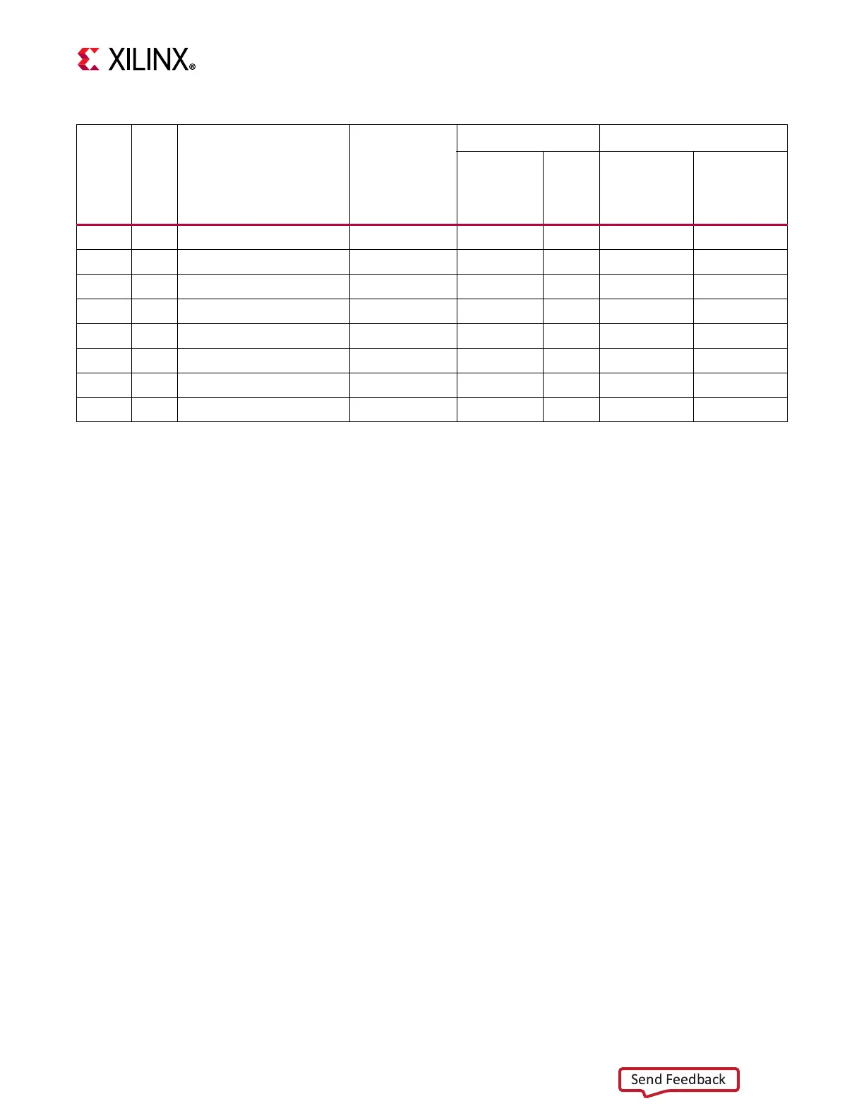
Table 2-38: Page-Translation Bit Ranges by Page Size
Page
Size
SIZE
TLBHI
Field
Tag Comparison
Bit Range
Page Offset
PAE Disabled PAE Enabled
1
Physical
Page
Number
RPN
Bits
Clear to
0
Physical Page
Number
RPN Bits
Clear to 0
1 KB 000 TAG[0:21] - Address[0:21] Address[22:31] RPN[0:21] - RPN[0:n-11] -
4 KB 001 TAG[0:19] - Address[0:19] Address[20:31] RPN[0:19] 20:21 RPN[0:n-13] n-12:n-11
16 KB 010 TAG[0:17] - Address[0:17] Address[18:31] RPN[0:17] 18:21 RPN[0:n-15] n-14:n-11
64 KB 011 TAG[0:15] - Address[0:15] Address[16:31] RPN[0:15] 16:21 RPN[0:n-17] n-16:n-11
256 KB 100 TAG[0:13] - Address[0:13] Address[14:31] RPN[0:13] 14:21 RPN[0:n-19] n-18:n-11
1 MB 101 TAG[0:11] - Address[0:11] Address[12:31] RPN[0:11] 12:21 RPN[0:n-21] n-20:n-11
4 MB 110 TAG[0:9] - Address[0:9] Address[10:31] RPN[0:9] 10:21 RPN[0:n-23] n-22:n-11
16 MB 111 TAG[0:7] - Address[0:7] Address[8:31] RPN[0:7] 8:21 RPN[0:n-25] n-24:n-11
1. The bit index n = C_ADDR_SIZE.