MicroBlaze Processor Reference Guide 63
UG984 (v2018.2) June 21, 2018 www.xilinx.com
Chapter 2: MicroBlaze Architecture
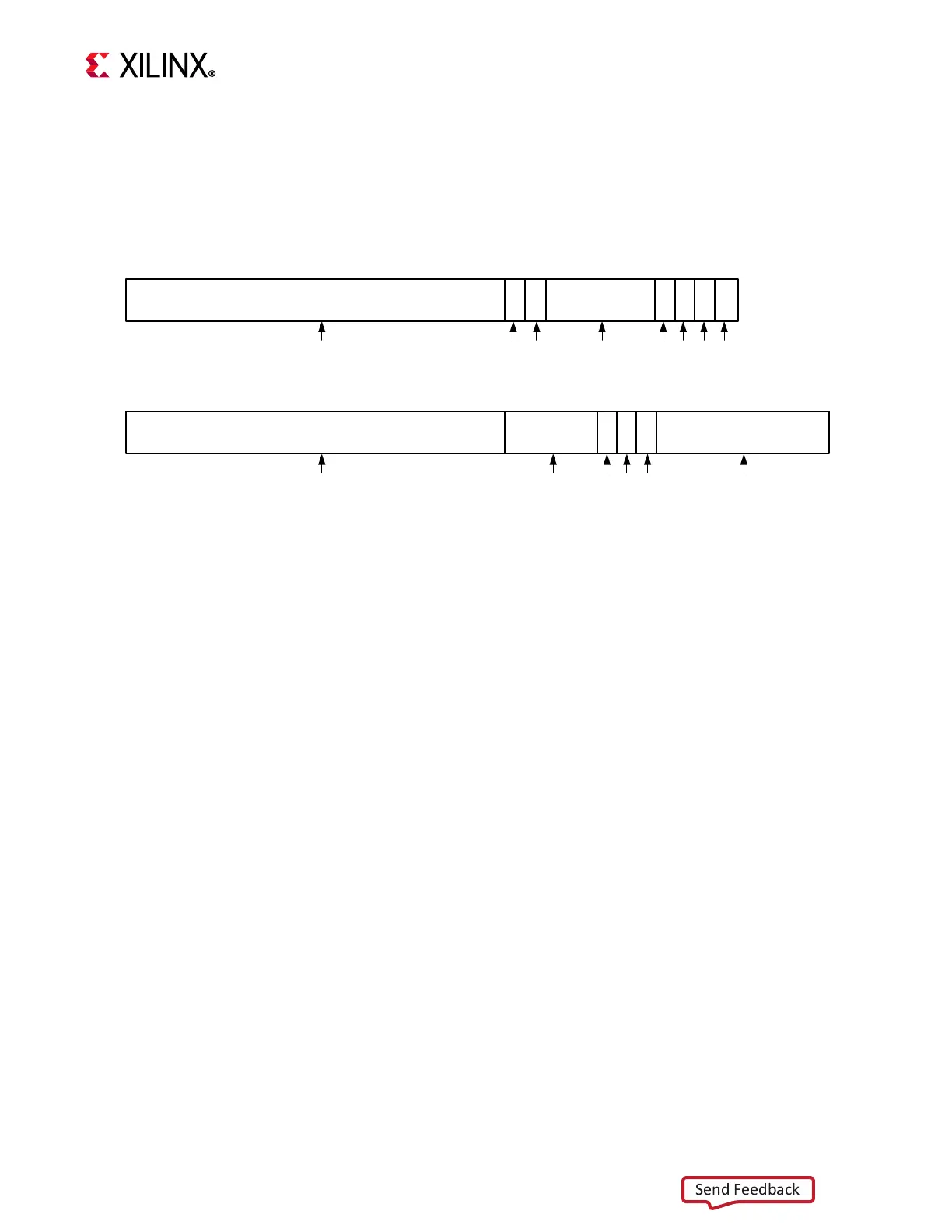
TLB Entry Format
The following figure shows the format of a TLB entry. Each TLB entry ranges from 68 bits up
to 100 bits and is composed of two portions: TLBLO (also referred to as the data entry), and
TLBHI (also referred to as the tag entry).
When the Physical Address Extension (PAE) is enabled, the TLB entry is extended with up to
32 additional bits in the TLBLO RPN field to support up to a 64 bit physical address.
The TLB entry contents are described in more detail in Table 2-20 and Table 2-21, including
the TLBLO format with PAE enabled.
The fields within a TLB entry are categorized as follows:
• Virtual-page identification (TAG, SIZE, V, TID): These fields identify the page-translation
entry. They are compared with the virtual-page number during the translation process.
• Physical-page identification (RPN, SIZE): These fields identify the translated page in
physical memory.
• Access control (EX, WR, ZSEL): These fields specify the type of access allowed in the
page and are used to protect pages from improper accesses.
• Storage attributes (W, I, M, G, E, U0): These fields specify the storage-control attributes,
such as caching policy for the data cache (write-back or write-through), whether a page
is cacheable, and how bytes are ordered (endianness).
Table 2-38 shows the relationship between the TLB-entry SIZE field and the translated
page size. This table also shows how the page size determines which address bits are
involved in a tag comparison, which address bits are used as a page offset, and which bits
in the physical page number are used in the physical address. With PAE enabled, the most
significant bits of the physical address are directly taken from the extended RPN field.
X-Ref Target - Figure 2-20
Figure 2-20: TLB Entry Format (PAE Disabled)
RPN
22
0
31
28
24
23
ZSEL
W I G
TAG
22
0
3528
272625
SIZE
V E TID
TLBLO:
TLBHI:
29
30
M
U0
EX
WR
X19757-091117