MicroBlaze Processor Reference Guide 40
UG984 (v2018.2) June 21, 2018 www.xilinx.com
Chapter 2: MicroBlaze Architecture
Note: The UTLB is not reset by the external reset inputs: Reset and Debug_Rst.
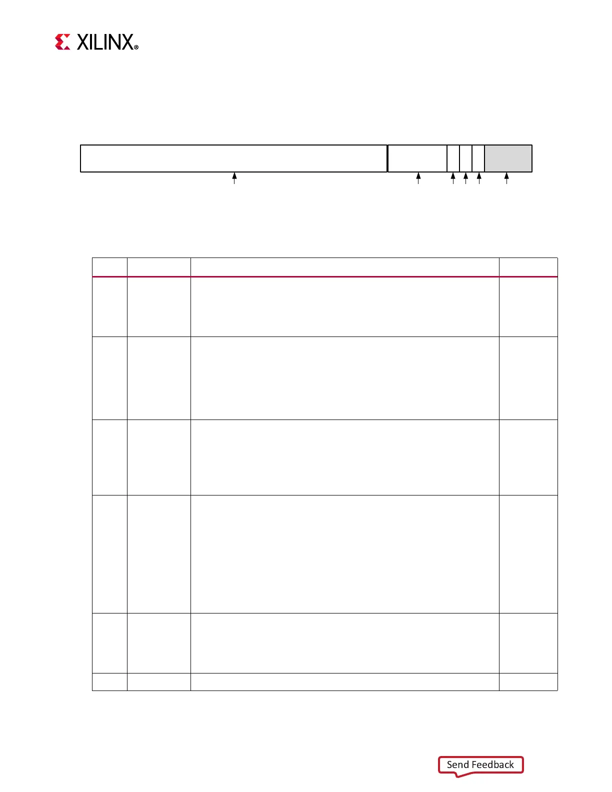
The following figure illustrates the TLBHI register and Table 2-21 provides bit descriptions
and reset values.
X-Ref Target - Figure 2-15
Figure 2-15: TLBHI
TAG
22
0
31
28
27
26
25
SIZE
V E U0 Reserved
X19752-091317
Table 2-21: Translation Look-Aside Buffer High Register (TLBHI)
Bits Name Description Reset Value
0:21 TAG TLB-entry tag
Is compared with the page number portion of the virtual memory
address under the control of the SIZE field.
Read/Write
0x000000
22:24 SIZE Size
Specifies the page size. The SIZE field controls the bit range used in
comparing the TAG field with the page number portion of the virtual
memory address. The page sizes defined by this field are listed in
Table 2-38.
Read/Write
000
25 V Valid
When this bit is set to 1, the TLB entry is valid and contains a page-
translation entry.
When cleared to 0, the TLB entry is invalid.
Read/Write
0
26 E Endian
When this bit is set to 1, the page is accessed as a big endian page.
When cleared to 0, the page is accessed as a little endian page.
The E bit only affects data read or data write accesses. Instruction
accesses are not affected.
The E bit is only implemented when the parameter
C_USE_REORDER_INSTR is set to 1, otherwise it is fixed to 0.
Read/Write
0
27 U0 User Defined
This bit is fixed to 0, since there are no user defined storage
attributes on MicroBlaze.
Read Only
0
28:31 Reserved