MicroBlaze Processor Reference Guide 38
UG984 (v2018.2) June 21, 2018 www.xilinx.com
Chapter 2: MicroBlaze Architecture
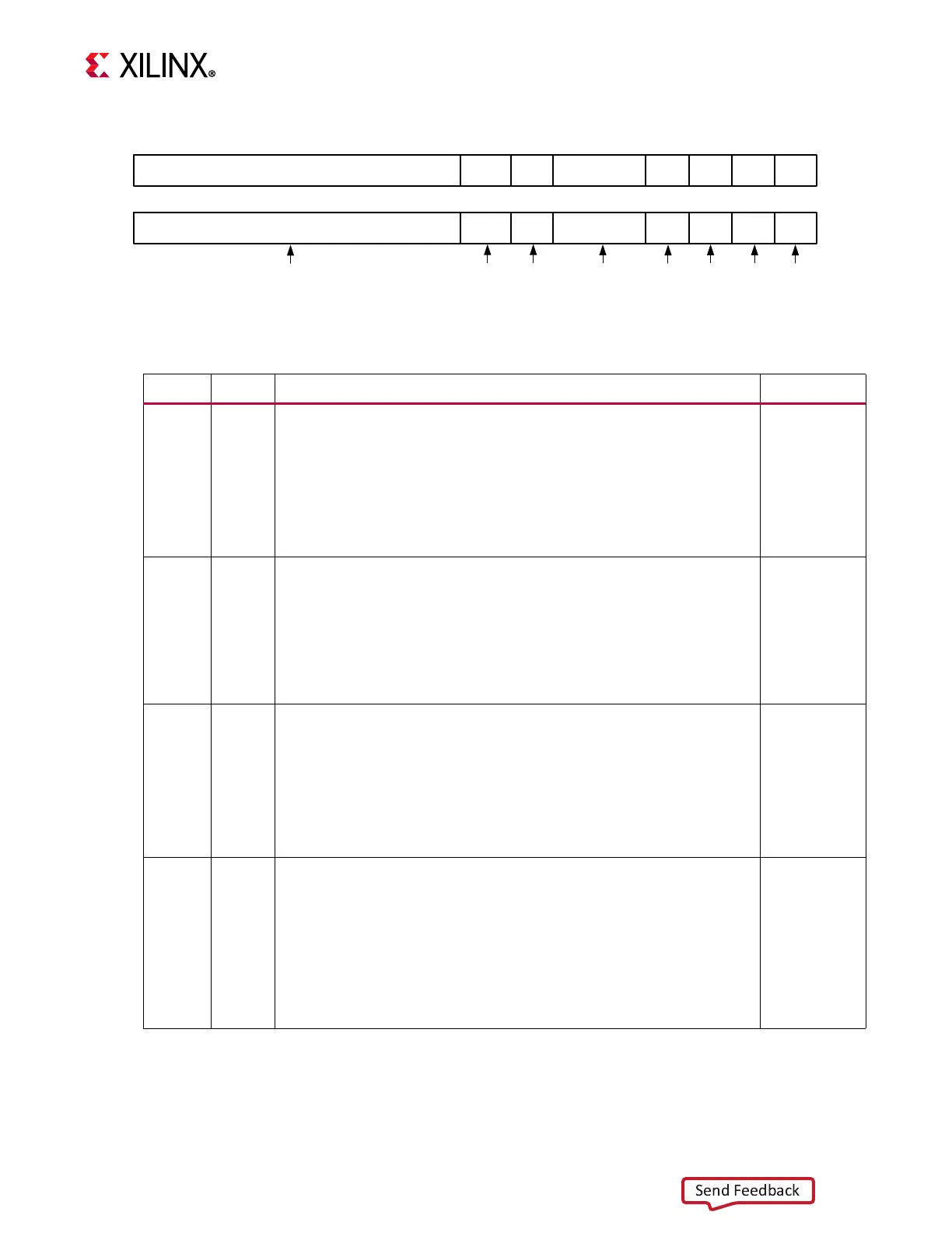
X-Ref Target - Figure 2-14
Figure 2-14: TLBLO
0
0
22
n-10 n-9 n-8
28
29
30
31
n-4
n-3 n-2 n-1
C_ADDR_SIZE = 32 or C_USE_MMU ≠ 3:
PAE: C_ADDR_SIZE > 32 and C_USE_MMU = 3 (n = C_ADDR_SIZE):
RPN
EX
W
WR
ZSEL I M
G
23 24
X19751-091317
Table 2-20: Translation Look-Aside Buffer Low Register (TLBLO)
Bits
1
Name Description Reset Value
0:21
0:n-11
RPN Real Page Number or Physical Page Number
When a TLB hit occurs, this field is read from the TLB entry and is
used to form the physical address. Depending on the value of the
SIZE field, some of the RPN bits are not used in the physical address.
Software must clear unused bits in this field to zero.
Only defined when C_USE_MMU=3 (Virtual).
Read/Write
0x000000
22
n-10
EX Executable
When bit is set to 1, the page contains executable code, and
instructions can be fetched from the page. When bit is cleared to 0,
instructions cannot be fetched from the page. Attempts to fetch
instructions from a page with a clear EX bit cause an instruction-
storage exception.
Read/Write
0
23
n-9
WR Writable
When bit is set to 1, the page is writable and store instructions can
be used to store data at addresses within the page.
When bit is cleared to 0, the page is read-only (not writable).
Attempts to store data into a page with a clear WR bit cause a data
storage exception.
Read/Write
0
24:27
n-8:n-5
ZSEL Zone Select
This field selects one of 16 zone fields (Z0-Z15) from the zone-
protection register (ZPR).
For example, if ZSEL 0x5, zone field Z5 is selected. The selected ZPR
field is used to modify the access protection specified by the TLB
entry EX and WR fields. It is also used to prevent access to a page by
overriding the TLB V (valid) field.
Read/Write
0x0