MicroBlaze Processor Reference Guide 62
UG984 (v2018.2) June 21, 2018 www.xilinx.com
Chapter 2: MicroBlaze Architecture
• Data Shadow TLB: The DTLB contains data page-translation entries and is fully
associative. The page-translation entries stored in the DTLB represent the most-recently
accessed data-page translations from the UTLB. The DTLB is used to minimize
contention between data translation and UTLB-update operations. The initialization
and management of the DTLB is controlled completely by hardware and is transparent
to software.
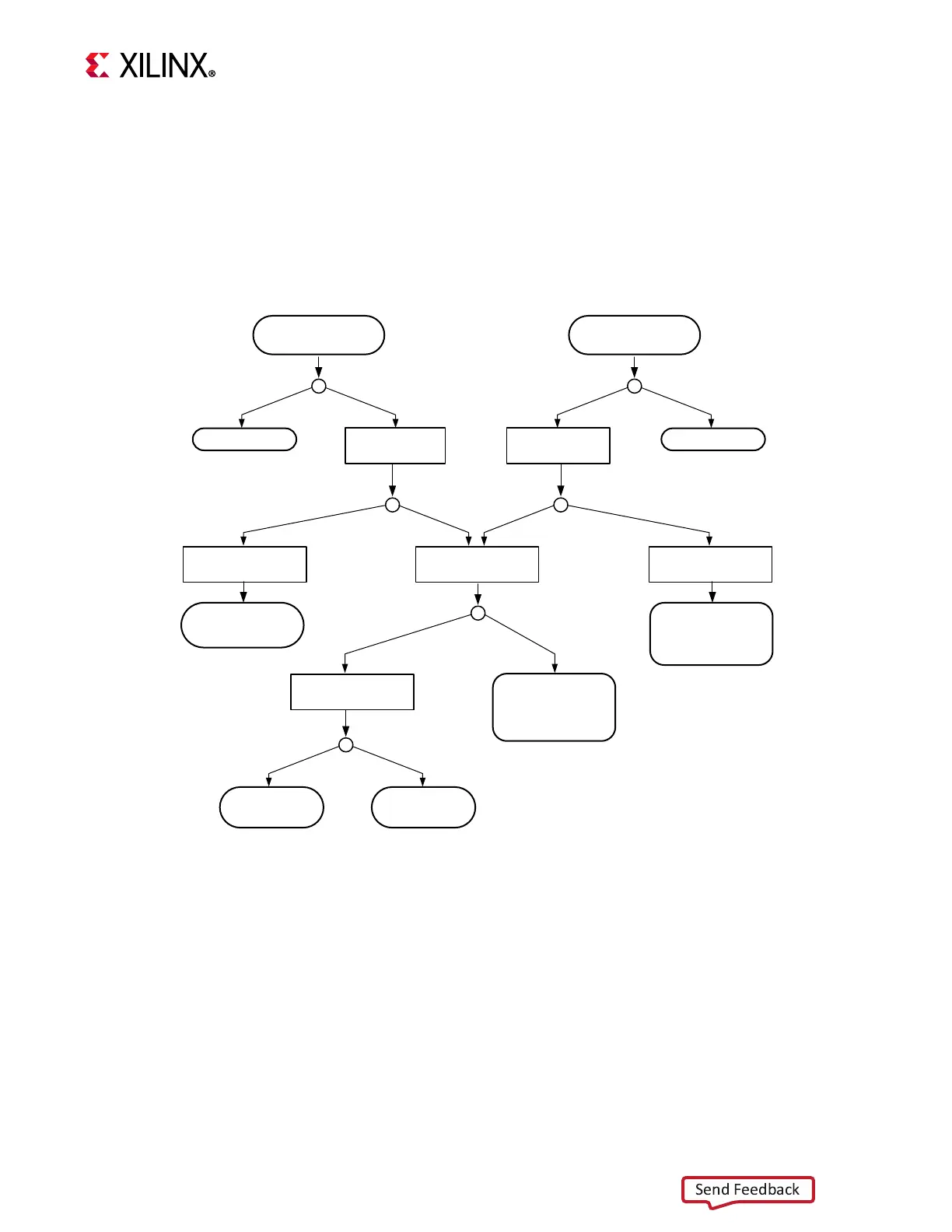
The following figure provides the translation flow for TLB.
X-Ref Target - Figure 2-19
Figure 2-19: TLB Address Translation Flow
Perform DTLB
Look-Up
Generate I-side
Effective Address
No Translation
Perform ITLB
Look-Up
Translation Disabled
(MSR[VM]=0)
Translation Enabled
(MSR[VM]=1)
Generate D-side
Effective Address
No Translation
Translation Enabled
(MSR[VM]=1)
Translation Disabled
(MSR[VM]=0)
ITLB Hit ITLB Miss DTLB Miss DTLB Hit
Extract Real
Address from ITLB
Perform UTLB
Look-Up
Extract Real
Address from DTLB
Continue I-cache
Access
Continue I-cache
or D-cache
Access
UTLB Hit UTLB Miss
Extract Real
Address from UTLB
I-Side TLB Miss or
D-Side TLB Miss
Exception
Route Address
to ITLB
Route Address
to DTLB
X19756-082517