MicroBlaze Processor Reference Guide 88
UG984 (v2018.2) June 21, 2018 www.xilinx.com
Chapter 2: MicroBlaze Architecture
The following table summarizes all types of accesses issued by the data cache AXI4
interface.
Victim Cache
The victim cache is enabled by setting the parameter C_DCACHE_VICTIMS to 2, 4 or 8. This
defines the number of cache lines that can be stored in the victim cache. Whenever a
complete cache line is evicted from the cache, it is saved in the victim cache. By saving the
most recent lines they can be fetched much faster, should the processor request them,
thereby improving performance. If the victim cache is not used, all evicted cache lines must
be read from memory again when they are needed.
With the AXI4 interface, C_DCACHE_DATA_WIDTH determines the amount of data transferred
from/to the victim cache each clock cycle, either 32 bits or an entire cache line.
Note: To be able to use the victim cache, write-back must be enabled and area optimization must
not be enabled.
Data Cache Software Support
MSR Bit
The DCE bit in the MSR controls whether or not the cache is enabled. When disabling
caches the user must ensure that all the prior writes within the cacheable range have been
completed in external memory before reading back over
M_AXI_DP. This can be done by
writing to a semaphore immediately before turning off caches, and then in a loop poll until
it has been written. The contents of the cache are preserved when the cache is disabled.
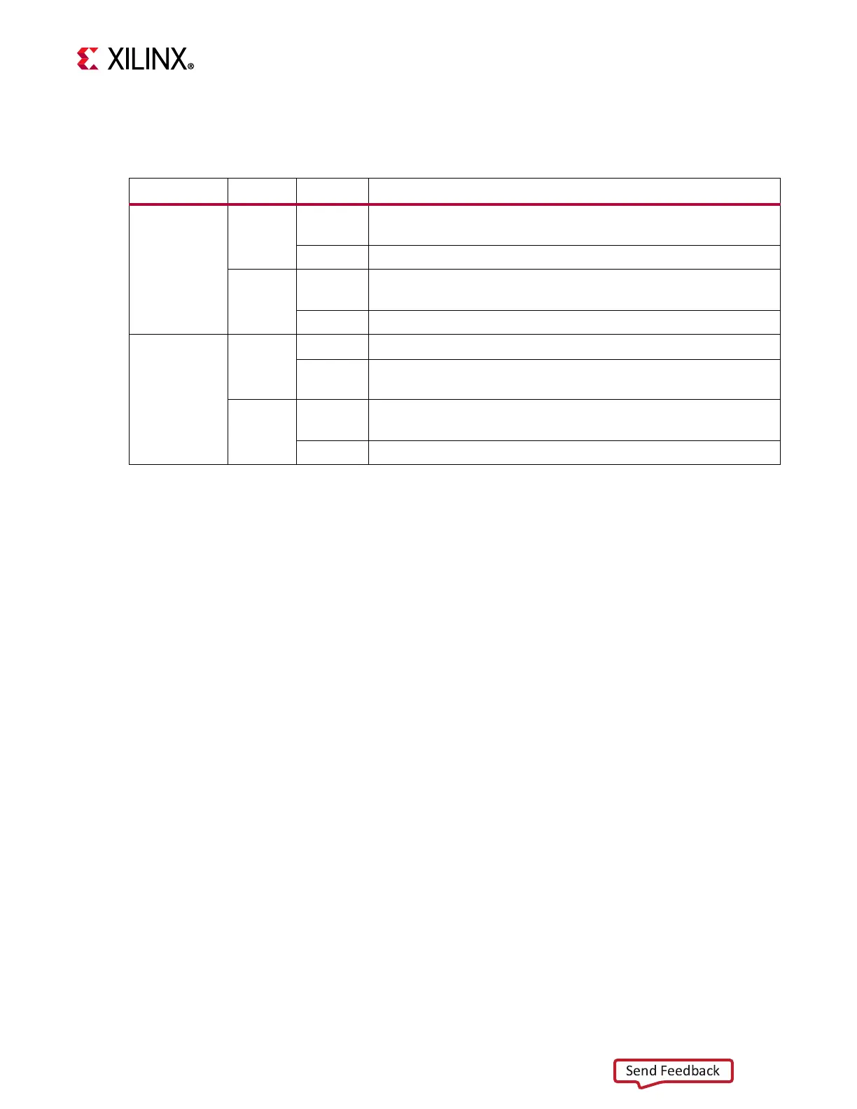
Table 2-40: Data Cache Interface Accesses
Policy State Direction Access Type
Write-
through
Cache
Enabled
Read Burst for 32-bit interface non-exclusive access and exclusive
access with ACE enabled, single access otherwise
Write Single access
Cache
Disabled
Read Burst for 32-bit interface exclusive access with ACE enabled,
single access otherwise
Write Single access
Write-back Cache
Enabled
Read Burst for 32-bit interface, single access otherwise
Write Burst for 32-bit interface cache lines with more than one valid
word, a single access otherwise
Cache
Disabled
Read Burst for 32-bit interface non-exclusive access, discarding all but
the desired data, a single access otherwise
Write Single access