MicroBlaze Processor Reference Guide 99
UG984 (v2018.2) June 21, 2018 www.xilinx.com
Chapter 2: MicroBlaze Architecture
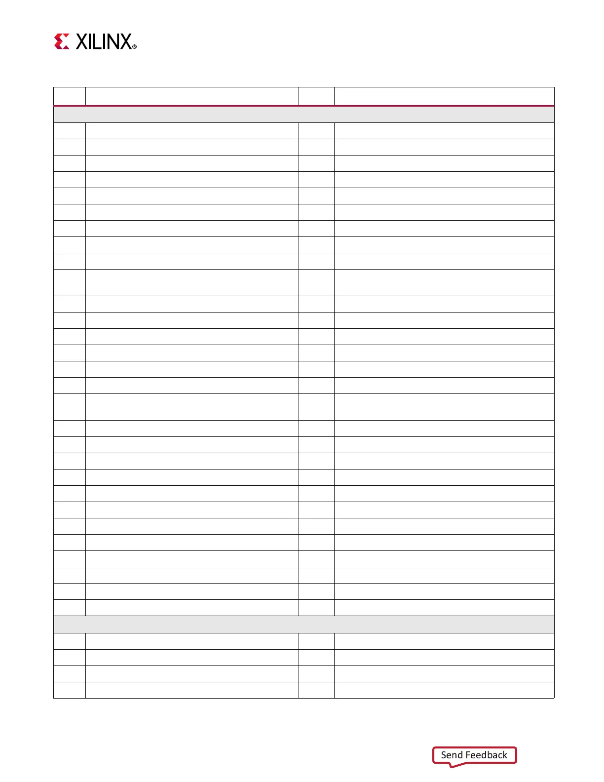
Table 2-41: MicroBlaze Performance Monitoring Events
Event Description Event Description
Event Counter Events
0 Any valid instruction executed 29 Floating-point (fadd, ..., fsqrt)
1 Load word (lw, lwi, lwx) executed 30 Number of clock cycles
2 Load halfword (lhu, lhui) executed 31 Immediate (imm) executed
3 Load byte (lbu, lbui) executed 32 Pattern compare (pcmpbf, pcmpeq, pcmpne)
4 Store word (sw, swi, swx) executed 33 Sign extend instructions (sext8, sext16) executed
5 Store halfword (sh, shi) executed 34 Instruction cache invalidate (wic) executed
6 Store byte (sb, sbi) executed 35 Data cache invalidate or flush (wdc) executed
7 Unconditional branch (br, bri, brk, brki) executed 36 Machine status instructions (msrset, msrclr)
8 Taken conditional branch (beq, ..., bnei) executed 37 Unconditional branch with delay slot executed
9 Not taken conditional branch (beq,..., bnei)
executed
38 Taken conditional branch with delay slot executed
10 Data request from instruction cache 39 Not taken conditional branch with delay slot
11 Hit in instruction cache 40 Delay slot with no operation instruction executed
12 Read data requested from data cache 41 Load instruction (lbu, ..., lwx) executed
13 Read data hit in data cache 42 Store instruction (sb, ..., swx) executed
14 Write data request to data cache 43 MMU data access request
15 Write data hit in data cache 44 Conditional branch (beq, ..., bnei) executed
16 Load (lbu, ..., lwx) with r1 as operand executed 45 Branch (br, bri, brk, brki, beq, ..., bnei)
executed
17 Store (sb, ..., swx) with r1 as operand executed 46 Read or write data request from/to data cache
18 Logical operation (and, andn, or, xor) executed 47 Read or write data cache hit
19 Arithmetic operation (add, idiv, mul, rsub) executed 48 MMU exception taken
20 Multiply operation (mul, mulh, mulhu, mulhsu, muli) 49 MMU instruction side exception taken
21 Barrel shifter operation (bsrl, bsra, bsll) executed 50 MMU data side exception taken
22 Shift operation (sra, src, srl) executed 51 Pipeline stalled
23 Exception taken 52 Branch target cache hit for a branch or return
24 Interrupt occurred 53 MMU instruction side access request
25 Pipeline stalled due to operand fetch stage (OF) 54 MMU instruction TLB (ITLB) hit
26 Pipeline stalled due to execute stage (EX) 55 MMU data TLB (DTLB) hit
27 Pipeline stalled due to memory stage (MEM) 56 MMU unified TLB (UTLB) hit
28 Integer divide (idiv, idivu) executed
Latency and Event Counter events
57 Interrupt latency from input to interrupt vector 61 MMU address lookup latency
58 Data cache latency for memory read 62 Peripheral AXI interface data read latency
59 Data cache latency for memory write 63 Peripheral AXI interface data write latency
60 Instruction cache latency for memory read