ZCU106 Board User Guide 41
UG1244 (v1.0) March 28, 2018 www.xilinx.com
Chapter 3: Board Component Descriptions
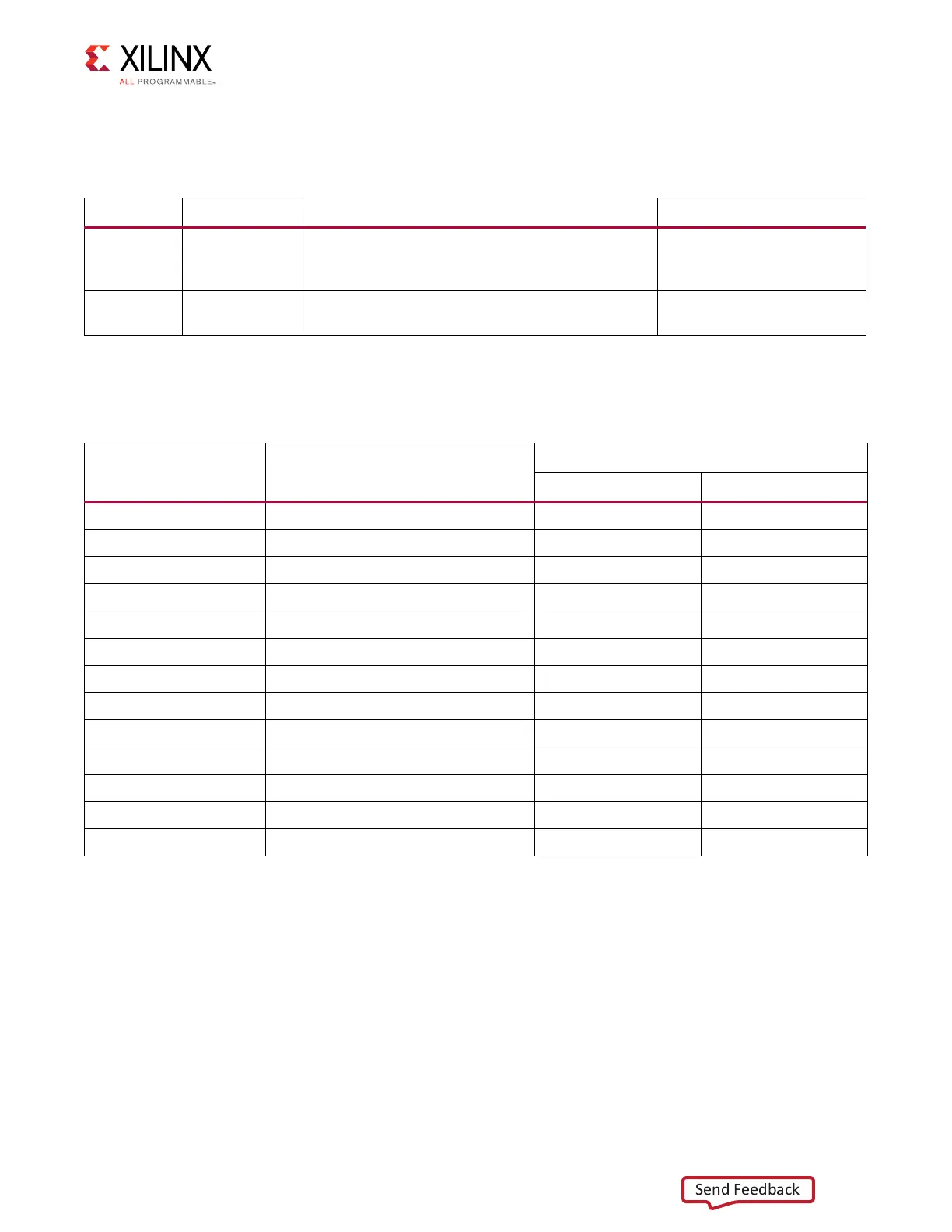
Table 3-7 describes the jumper settings for the USB 2.0 circuit. Bold text identifies the
default shunt positions for USB 2.0 high speed on-the-go (OTG) mode.
The connections between the USB 2.0 PHY at U116 and the XCZU7EV MPSoC are listed in
Table 3-8.
Note:
The shield for the USB 3.0 A connector (J96) can be tied to GND by a jumper on header J112
pins 2-3 (default). The USB shield can optionally be connected through a capacitor to GND by
installing a capacitor (body size 0402) at location C887 and jumping pins 1-2 on header J112.
Table 3-7: USB Jumper Settings
Header Function Shunt Position Notes
J110 CVBUS select
ON = Device mode (1 µF)
OFF = Host mode (120 µF) and source of bus
power
VBUS load capacitance
J96 USB 3.0 A
Position 1-2 = Shield floating (DNP C887 pads)
Position 2-3 = Shield connected to GND
Table 3-8: USB 2.0 ULPI Transceiver Connections to the XCZU7EV MPSoC
XCZU7EV (U1) Pin Net Name
USB3320 U116
Pin # Pin Name
U117.4 ULPI0_RST_B
(1)
27 RESET_B
H31 MIO58_USB_STP
(2)
29 STP
G30 MIO53_USB_DIR 31 DIR
G29 MIO52_USB_CLK 1 CLKOUT
G33 MIO55_USB_NXT 2 NXT
G34 MIO56_USB_DATA0
(2)
3 DATA0
H29 MIO57_USB_DATA1
(2)
4 DATA1
G31 MIO54_USB_DATA2
(2)
5 DATA2
H32 MIO59_USB_DATA3
(2)
6 DATA3
H33 MIO60_USB_DATA4
(2)
7 DATA4
H34 MIO61_USB_DATA5
(2)
9 DATA5
J29 MIO62_USB_DATA6
(2)
10 DATA6
J30 MIO63_USB_DATA7
(2)
13 DATA7
Notes:
1. PS_POR_B (U1.M24) or PS_MODE1 (DIP SW6.2) or PB SW2 drive U116 RST_B via OR gate U117.
2. These nets are 30Ω series resistor coupled.