ZCU106 Board User Guide 49
UG1244 (v1.0) March 28, 2018 www.xilinx.com
Chapter 3: Board Component Descriptions
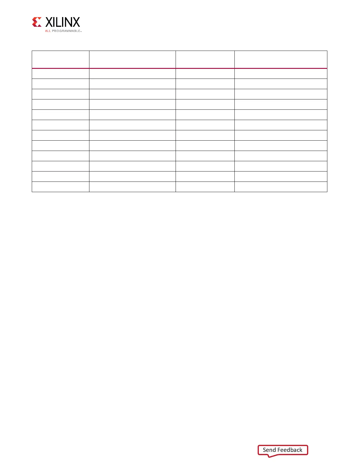
U56.4 USER_MGT_SI570_P
(2)
(1-to-2 CLOCK BUFFER) U51.6
U56.5 USER_MGT_SI570_N
(2)
(1-to-2 CLOCK BUFFER) U51.7
U51.11 USER_MGT_SI570_CLOCK1_P
(2)
U10
U51.12 USER_MGT_SI570_CLOCK1_N
(2)
U9
U51.13 USER_MGT_SI570_CLOCK2_P
(2)
R10
U51.14 USER_MGT_SI570_CLOCK2_N
(2)
R9
J79.1 USER_SMA_MGT_CLOCK_P
(2)
AA10
J80.1 USER_SMA_MGT_CLOCK_N
(2)
AA9
U108.28 HDMI_SI5324_OUT_P
(2)
AD8
U108.29 HDMI_SI5324_OUT_N
(2)
AD7
U20.28 SFP_SI5328_OUT_P
(2)
W10
U20.29 SFP_SI5328_OUT_N
(2)
W9
Notes:
1. U1 XCU7EV Bank 503 supports LVCMOS level inputs.
2. U1 MGT (I/O standards do not apply).
Table 3-13: Clock Connections, Source to XCZU7EV MPSoC (Cont’d)
Clock Source Ref.
Des. and Pin
Net Name I/O Standard XCZU7EV (U1) Pin
 Loading...


