ZCU106 Board User Guide 51
UG1244 (v1.0) March 28, 2018 www.xilinx.com
Chapter 3: Board Component Descriptions
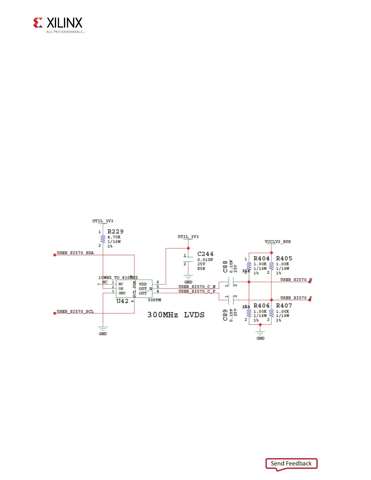
Programmable User Clock
[Figure 2-1, callout 9]
The ZCU106 board has an I2C programmable SI570 low-jitter 3.3V LVDS differential
oscillator (U42) connected to the GC inputs of PL bank 66. This USER_SI570_P and
USER_SI570_N clock signals are connected to XCZU7EV MPSoC U1 pins AH12 and AJ12,
respectively. On power up, the user clock defaults to an output frequency of 300.000 MHz.
User applications can change the output frequency within the range of 10 MHz to 810 MHz
through an I2C interface. Power cycling the ZCU106 board reverts this user clock to the
default frequency of 300.000 MHz.
This oscillator can be reprogrammed from MSP430 system controller U41 (see TI MSP430
System Controller, page 116 for more information).
• Programmable oscillator: Silicon Labs Si570BAB001614DG (10 MHz-810 MHz, 300 MHz
default)
• LVDS differential output
• Total stability: 61.5 ppm
X-Ref Target - Figure 3-9
Figure 3-9: Programmable User Clock

 Loading...


