15.3 External clock (XCK)
External clocking is used by the synchronous or SPI slave modes of operation. External clock input
from the XCK pin is sampled by a synchronization logic to remove meta-stability. The output from the
synchronization logic must then pass through an edge detector before it can be used by Transmitter
and Receiver.
This process introduces a two CPU clock period delay and the maximum frequency of the external XCK
pin is limited by the following equation:
fXCK =
fSCLK
4
, where fXCK is the frequency of XCK, and fSCLK is the frequency of main system clock (SCLK).
15.4 Synchronous mode operation
When synchronous mode or SPI mode is used, the XCK pin will be used as either clock input (slave)
or clock output (master). The dependency between a clock edge and data sampling or data change is
the same. The basic principle is that data input on RXD (MISO in SPI mode) pin is sampled at the
opposite XCK clock edge at the edge in the data output on TXD (MOSI in SPI mode) pin is changed.
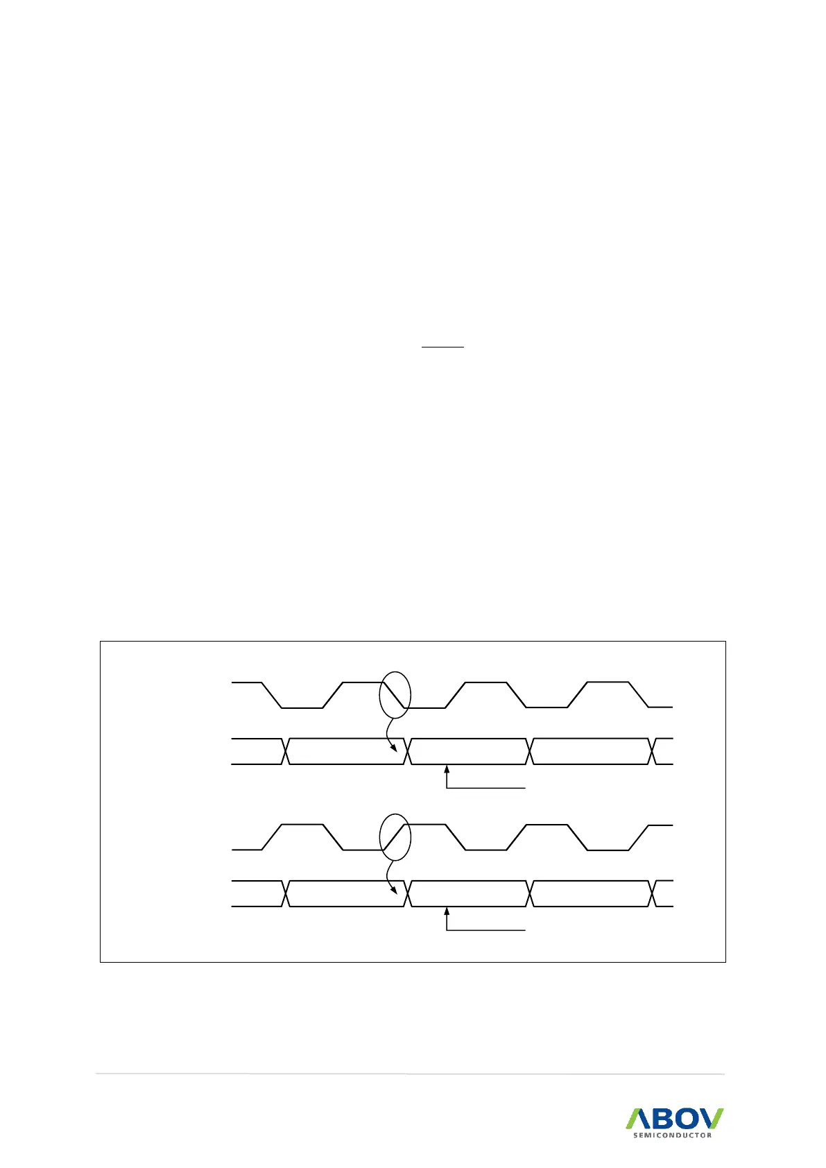
UCPOL bit in UCTRL1 register selects which XCK clock edge is used for data sampling and which is
used for data change. As shown in Figure 68, when UCPOL is zero, data will be changed at XCK rising
edge and sampled at XCK falling edge.