MC97F6108A User’s manual 23. Development tools
23.4 Flash programming
Program memory of MC97F6108A is a Flash type. This Flash ROM is accessed through four pins such
as DSCL, DSDA, VDD, and VSS in serial data format. For more information about Flash memory
programming, please refer to 19. Memory programming.
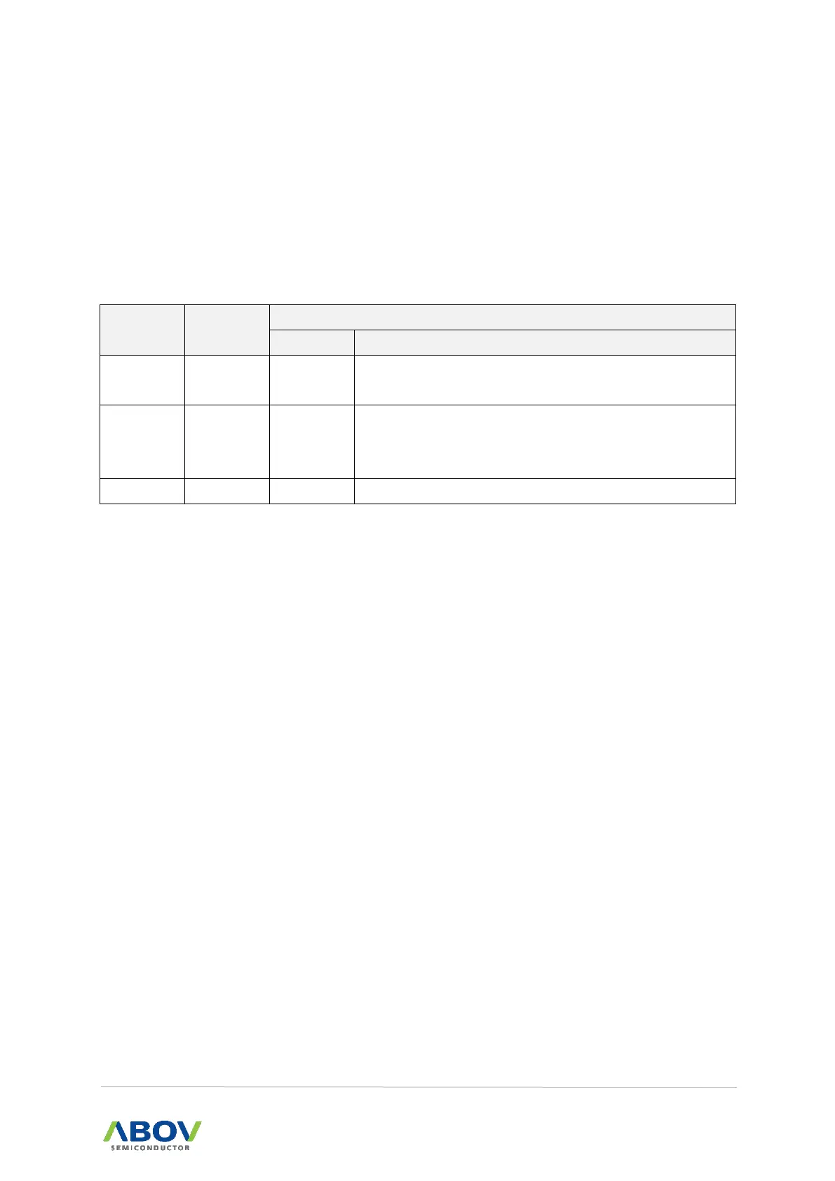
Table 58 introduces each pin and corresponding I/O status.
Table 58. Pins for Flash Programming
Serial clock pin. Input only pin.
Serial data pin. Output port when reading and input port
when programming. Can be assigned as input/push-pull
output port.
23.4.1 On-board programming
A31G32x need only four signal lines including VDD and VSS pins for programming Flash ROM with
serial protocol. Therefore, the on-board programming is possible if the programming signal lines are
considered when the PCB of application board is designed.