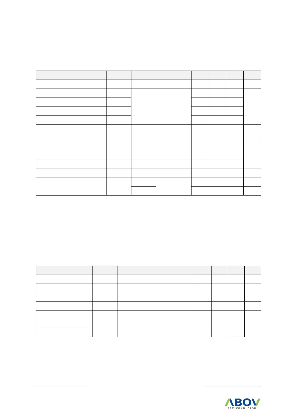
20.6 A/D Converter characteristics
Table 43. A/D Converter Characteristics
(T
A
=-40°C ~ +85°C, VDD=2.7V ~ 5.5V, VSS=0V)
NOTES:
1. Zero offset error is the difference between 000000000000 and the converted output for zero input voltage
(VSS).
2. Full scale error is the difference between 111111111111 and the converted output for full-scale input
voltage (AVREF).
3. When AVREF is lower than 2.7V, the ADC resolution is worse.
20.7 Low voltage reset characteristics
Table 44. Low Voltage Reset Characteristics
(T
A
=-40°C ~ +85°C, VDD=2.7V ~ 5.5V, VSS=0V)