23. Development tools MC97F6108A User’s manual
23.4.2 Circuit design guide
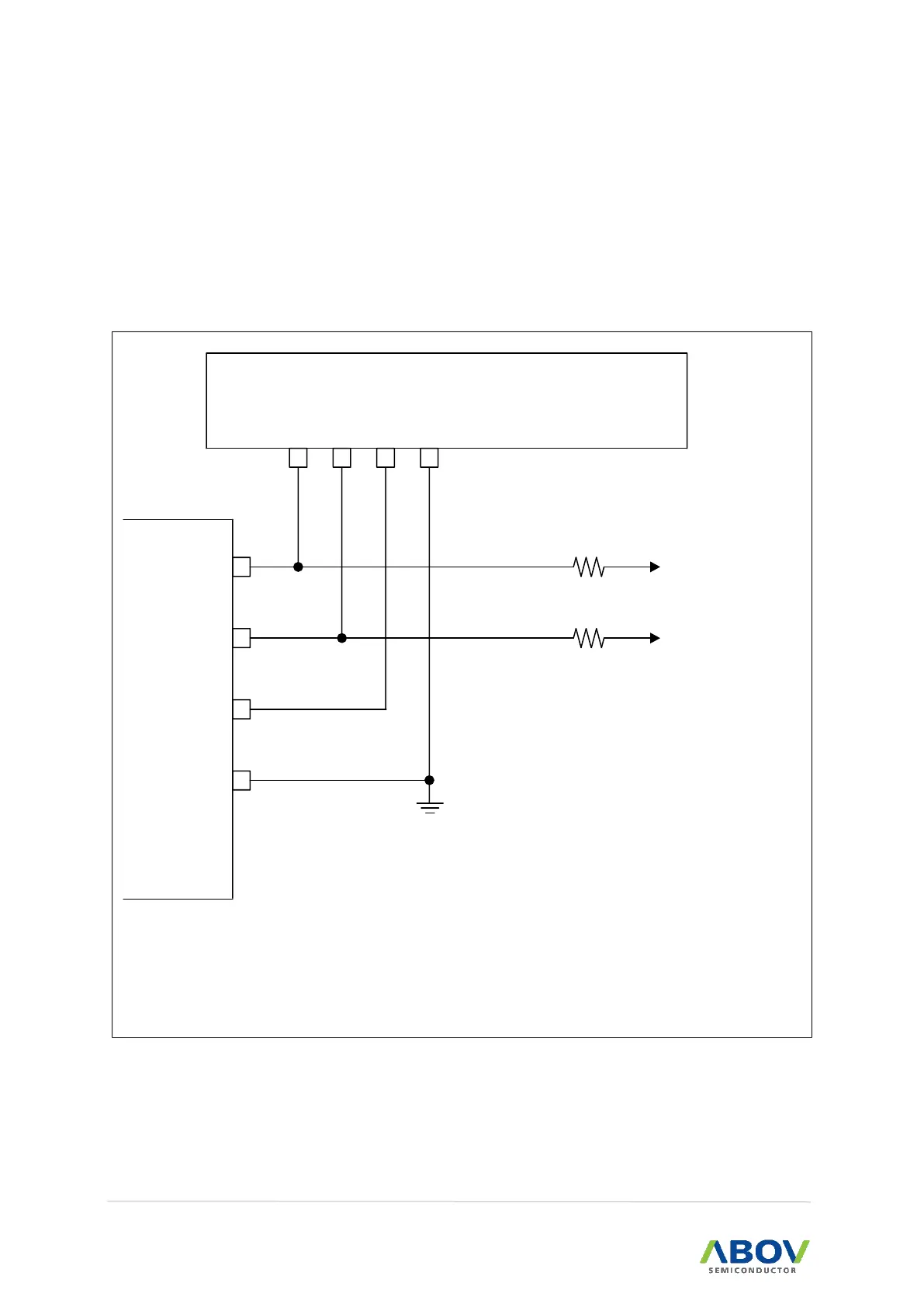
When programming Flash memory, the programming tool needs 4 signal lines, DSCL, DSDA, VDD,
and VSS. If a user designs a PCB circuit, the user should consider the usage of these 4 signal lines for
the on-board programming.
Please be careful to design the related circuit of these signal pins because rising/falling timing of DSCL
and DSDA is very important for proper programming.
To application circuitDSCL(I)
DSDA(I/O)
R1 (2k ~ 5k)
To application circuit
R2 (2k ~ 5k)
VDD
VSS
E-PGM+ , E-GANG4 , E-GANG6
NOTES:
1. In on-board programming mode, very high-speed signal will be provided to pin DSCL and DSDA.
And it will cause some damages to the application circuits connected to DSCL or DSDA port if the
application circuit is designed as high speed response such as relay control circuit. If possible, the
I/O configuration of DSDA, DSCL pins had better be set to input mode.
2. The value of R1 and R2 is recommended value. It varies with circuit of system.
Figure 125. PCB Design Guide for On-Board Programming
 Loading...


