EasyManuals Logo

Abov MC97F6108A User Manual

Default Icon
256 pages
To Next Page IconTo Next Page
To Previous Page IconTo Previous Page
Page #17 background imageLoading...
Page #17 background image
MC97F6108A User’s manual 2. Pinouts and pin description
17
2.2 Pin description
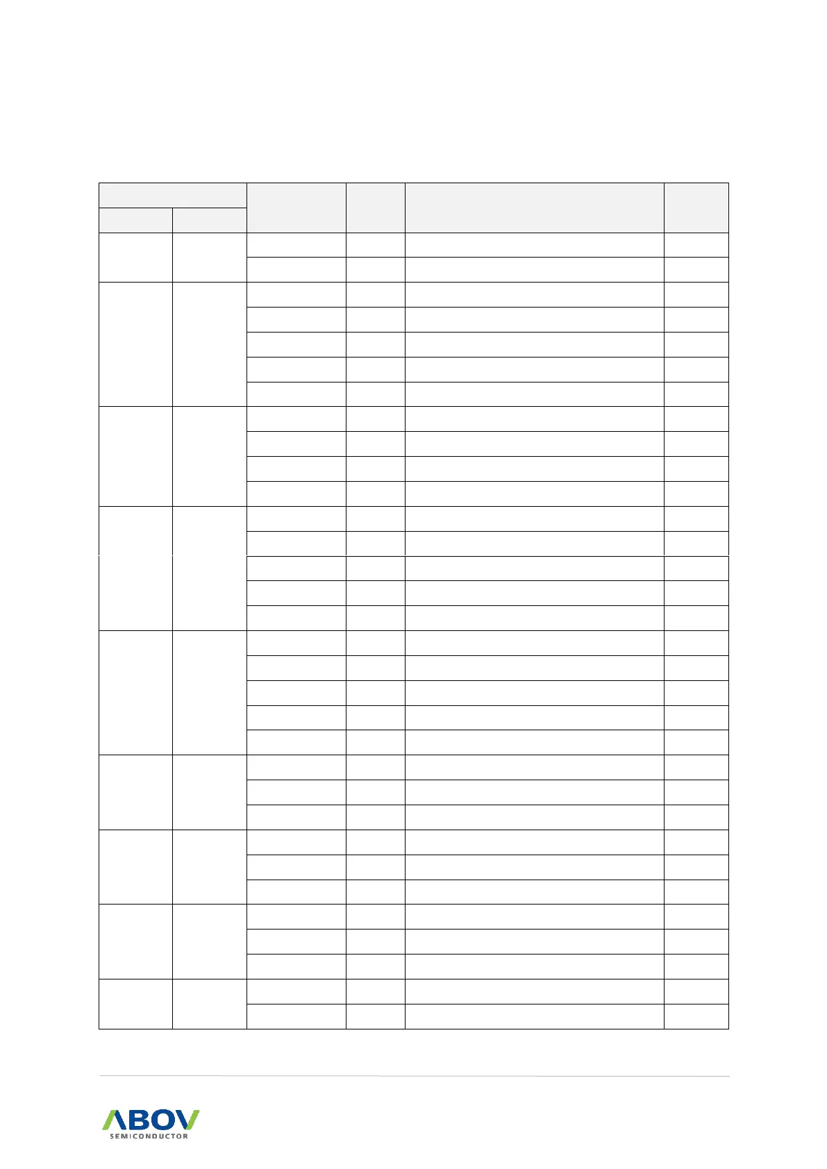
Table 2. Normal Pin Description
Pin no.
PIN Name
I/O
(1)
Description
Remark
20 SOP
16 SOPN
2
-
P00*
IOUS
Port 0 bit 0 Input/output
RSTB
IU
Reset pin
Pull-up
3
2
P01*
IOUS
Port 0 bit 1 Input/output
XCK
IO
USART clock signal
EC1
I
Timer 1(Event Capture) input
AN0
IA
ADC input ch-0
DSDA
IOU
OCD debugger data input/output
Pull-up
4
3
P02*
IOUS
Port 0 bit 2 Input/output
EINT0
I
External interrupt input ch-0
AN1
IA
ADC input ch-1
DSCL
IOU
OCD debugger clock
Pull-up
5
4
P03*
IOUS
Port 0 bit 3 Input/output
RXD
I
USART data receive
SDA
IO
I2C data signal
EINT1
I
External interrupt input ch-1
AN2
IA
ADC input ch-2
6
5
P04*
IOUS
Port 0 bit 4 Input/output
TXD
O
USART data transmit/SPI MOSI
SCL
IO
I2C clock signal
EINT2
I
External interrupt input ch-2
AN3
IA
ADC input ch-3
7
6
P05*
IOUS
Port 0 bit 5 Input/output
T3O
O
Timer 3 interval output
PPGO
O
Program pulse generator output
8
7
P06*
IOUS
Port 0 bit 6 Input/output
T1O
O
Timer 1 interval output
AN4
IA
ADC input ch-4
9
8
P07*
IOUS
Port 0 bit 7 Input/output
T0O
O
Timer 0 interval output
BUZO
O
Buzzer Output
10
-
P10*
IOUS
Port 1 bit 0 Input/output
EC0
I
Timer/Event Counter 0 input

Table of Contents

Questions and Answers:

Question and Answer IconNeed help?

Do you have a question about the Abov MC97F6108A and is the answer not in the manual?

Abov MC97F6108A Specifications

General IconGeneral
BrandAbov
ModelMC97F6108A
CategoryMicrocontrollers
LanguageEnglish

Related product manuals