162
2467S–AVR–07/09
ATmega128
When the modulator is enabled the type of modulation (logical AND or OR) can be selected by
the PORTB7 Register. Note that the DDRB7 controls the direction of the port independent of the
COMnx1:0 bit setting.
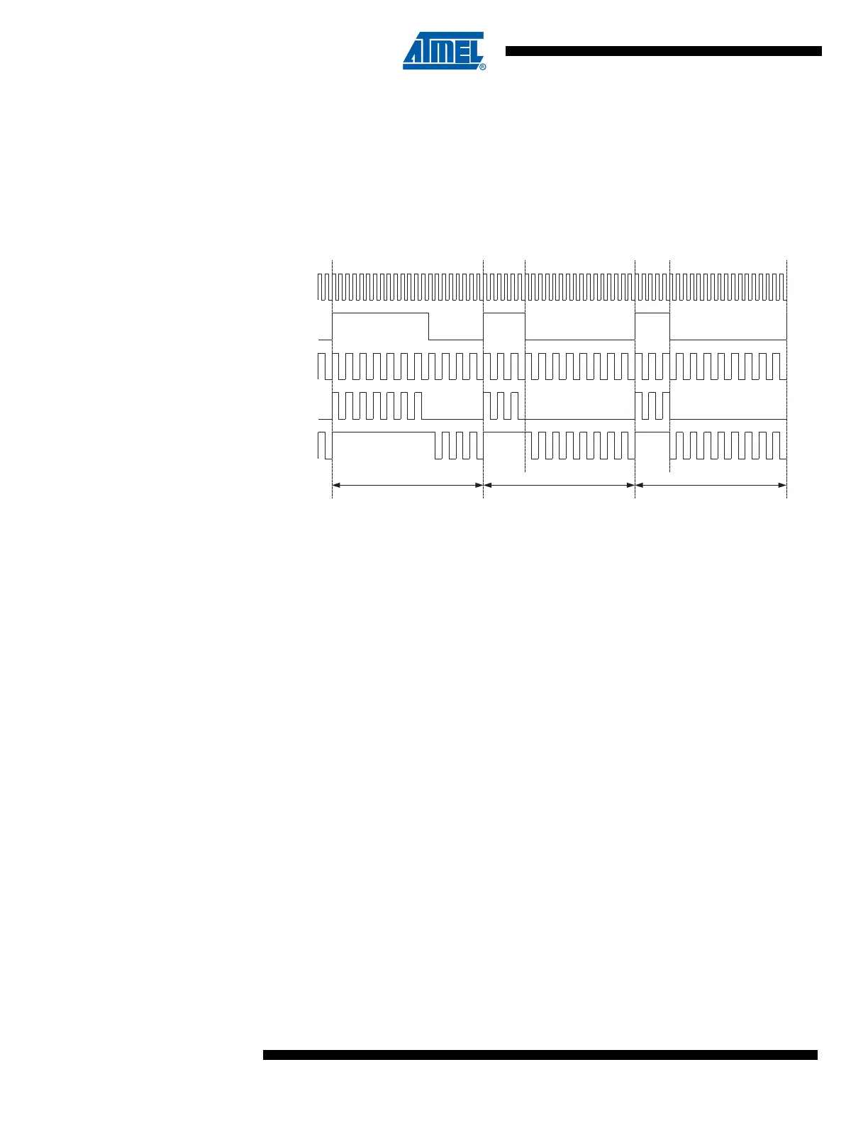
Timing Example Figure 74 illustrates the modulator in action. In this example the Timer/Counter1 is set to operate
in fast PWM mode (non-inverted) and Timer/Counter2 uses CTC waveform mode with toggle
Compare Output mode (COMnx1:0 = 1).
Figure 74. Output Compare Modulator, Timing Diagram
In this example, Timer/Counter2 provides the carrier, while the modulating signal is generated
by the Output Compare unit C of the Timer/Counter1.
The resolution of the PWM signal (OC1C) is reduced by the modulation. The reduction factor is
equal to the number of system clock cycles of one period of the carrier (OC2). In this example
the resolution is reduced by a factor of two. The reason for the reduction is illustrated in Figure
74 at the second and third period of the PB7 output when PORTB7 equals zero. The period 2
high time is one cycle longer than the period 3 high time, but the result on the PB7 output is
equal in both periods.
1 2
OC2
(CTC Mode)
OC1C
(FPWM Mode)
PB7
(PORTB7 = 0)
PB7
(PORTB7 = 1)
(Period)
3
clk
I/O