164
2467S–AVR–07/09
ATmega128
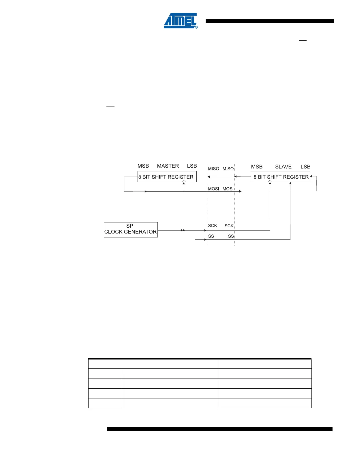
When configured as a Master, the SPI interface has no automatic control of the SS line. This
must be handled by user software before communication can start. When this is done, writing a
byte to the SPI Data Register starts the SPI clock generator, and the hardware shifts the 8 bits
into the Slave. After shifting one byte, the SPI clock generator stops, setting the end of transmis-
sion flag (SPIF). If the SPI interrupt enable bit (SPIE) in the SPCR Register is set, an interrupt is
requested. The Master may continue to shift the next byte by writing it into SPDR, or signal the
end of packet by pulling high the Slave Select, SS
line. The last incoming byte will be kept in the
buffer register for later use.
When configured as a Slave, the SPI interface will remain sleeping with MISO tri-stated as long
as the SS
pin is driven high. In this state, software may update the contents of the SPI Data
Register, SPDR, but the data will not be shifted out by incoming clock pulses on the SCK pin
until the SS
pin is driven low. As one byte has been completely shifted, the end of transmission
flag, SPIF is set. If the SPI interrupt enable bit, SPIE, in the SPCR Register is set, an interrupt is
requested. The Slave may continue to place new data to be sent into SPDR before reading the
incoming data. The last incoming byte will be kept in the buffer register for later use.
Figure 76. SPI Master-Slave Interconnection
The system is single buffered in the transmit direction and double buffered in the receive direc-
tion. This means that bytes to be transmitted cannot be written to the SPI Data Register before
the entire shift cycle is completed. When receiving data, however, a received character must be
read from the SPI Data Register before the next character has been completely shifted in. Oth-
erwise, the first byte is lost.
In SPI Slave mode, the control logic will sample the incoming signal of the SCK pin. To ensure
correct sampling of the clock signal, the minimum low and high period should be:
Low period: Longer than 2 CPU clock cycles.
High period: Longer than 2 CPU clock cycles.
When the SPI is enabled, the data direction of the MOSI, MISO, SCK, and SS
pins is overridden
according to Table 69. For more details on automatic port overrides, refer to “Alternate Port
Functions” on page 71.
Table 69. SPI Pin Overrides
(1)
Pin Direction, Master SPI Direction, Slave SPI
MOSI User Defined Input
MISO Input User Defined
SCK User Defined Input
SS User Defined Input