255
7647H–AVR–03/12
Atmel ATmega16/32/64/M1/C1
18.11.2 Amplifier 1 Control and Status register – AMP1CSR
• Bit 7 – AMP1EN: Amplifier 1 Enable Bit
Set this bit to enable the Amplifier 1.
Clear this bit to disable the Amplifier 1.
Clearing this bit while a conversion is running will take effect at the end of the conversion.
Warning: Always clear AMP1TS0:1 when clearing AMP1EN.
• Bit 6 – AMP1IS: Amplifier 1 Input Shunt
Set this bit to short-circuit the Amplifier 1 input.
Clear this bit to normally use the Amplifier 1.
• Bit 5, 4 – AMP1G1, 0: Amplifier 1 Gain Selection Bits
These 2 bits determine the gain of the amplifier 1.
The different setting are shown in Table 18-10.
To ensure an accurate result, after the gain value has been changed, the amplifier input needs
to have a quite stable input value during at least 4 Amplifier synchronization clock periods.
Table 18-9. AMP0 Clock Source Selection
AMP0TS2 AMP0TS1 AMP0TS0 Clock Source
0 0 0 ADC Clock/8
0 0 1 Timer/Counter0 Compare Match
0 1 0 Timer/Counter0 Overflow
0 1 1 Timer/Counter1 Compare Match B
1 0 0 Timer/Counter1 Overflow
1 0 1 PSC Module 0 Synchronization Signal (PSS0)
1 1 0 PSC Module 1 Synchronization Signal (PSS1)
1 1 1 PSC Module 2 Synchronization Signal (PSS2)
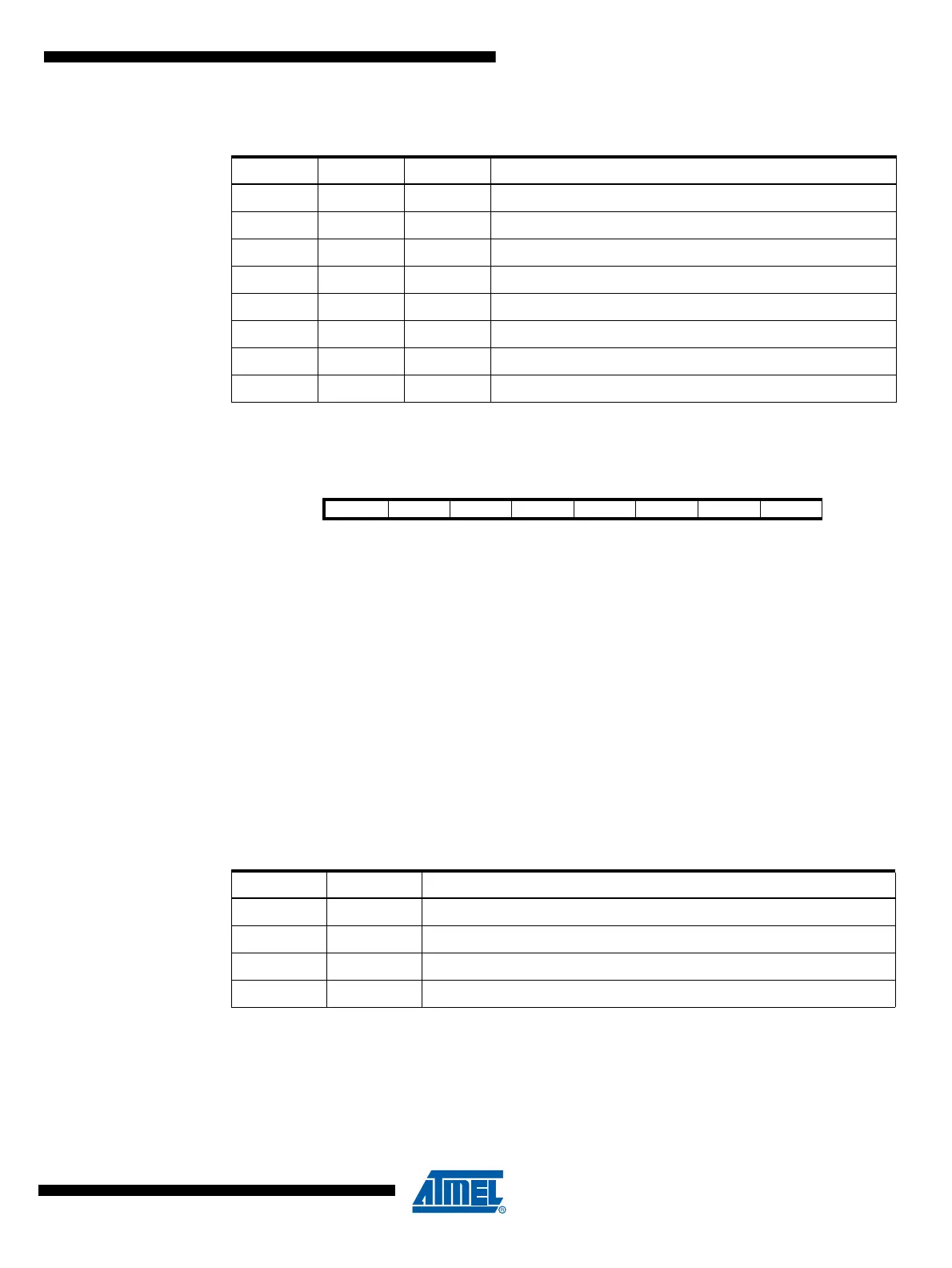
Bit 76543210
AMP1EN AMP1IS AMP1G1 AMP1G0 AMPCMP1 AMP1TS2 AMP1TS1 AMP1TS0 AMP1CSR
Read/Write R/W R/W R/W R/W R/W R/W R/W R/W
Initial Value 0 0 0 0 0 0 0 0
Table 18-10. Amplifier 1 Gain Selection
AMP1G1 AMP1G0 Description
00Gain 5
01Gain 10
10Gain 20
11Gain 40