256
7647H–AVR–03/12
Atmel ATmega16/32/64/M1/C1
• Bit 3 – AMPCMP1: Amplifier 1 - Comparator 1 connection
Set this bit to connect the amplifier 1 to the comparator 1 positive input. In this configuration the
comparator clock is twice amplifier clock.
Clear this bit to normally use the Amplifier 1.
• Bit 2:0 – AMP1TS2,AMP1TS1, AMP1TS0: Amplifier 1 Clock Source Selection Bits
In accordance with the Table 18-11, these 3 bits select the event which will generate the clock
for the amplifier 1. This clock source is necessary to start the conversion on the amplified
channel.
18.11.3 Amplifier 2 Control and Status register – AMP2CSR
• Bit 7 – AMP2EN: Amplifier 2 Enable Bit
Set this bit to enable the Amplifier 2.
Clear this bit to disable the Amplifier 2.
Clearing this bit while a conversion is running will take effect at the end of the conversion.
Warning: Always clear AMP2TS0:1 when clearing AMP2EN.
• Bit 6 – AMP2IS: Amplifier 2 Input Shunt
Set this bit to short-circuit the Amplifier 2 input.
Clear this bit to normally use the Amplifier 2.
• Bit 5, 4 – AMP2G1, 0: Amplifier 2 Gain Selection Bits
These 2 bits determine the gain of the amplifier 2.
The different setting are shown in Table 18-12.
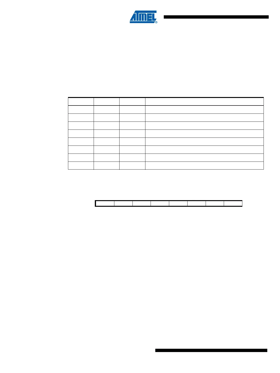
Table 18-11. AMP1 Clock Source Selection
AMP1TS2 AMP1TS1 AMP1TS0 Clock Source
0 0 0 ADC Clock/8
0 0 1 Timer/Counter0 Compare Match
0 1 0 Timer/Counter0 Overflow
0 1 1 Timer/Counter1 Compare Match B
1 0 0 Timer/Counter1 Overflow
1 0 1 PSC Module 0 Synchronization Signal (PSS0)
1 1 0 PSC Module 1 Synchronization Signal (PSS1)
1 1 1 PSC Module 2 Synchronization Signal (PSS2)
Bit 76543210
AMP2EN AMP2IS AMP2G1 AMP2G0 AMPCMP2 AMP2TS2 AMP2TS1 AMP2TS0 AMP2CSR
Read/Write R/W R/W R/W R/W R/W R/W R/W R/W
Initial Value 00000000