257
7647H–AVR–03/12
Atmel ATmega16/32/64/M1/C1
To ensure an accurate result, after the gain value has been changed, the amplifier input needs
to have a quite stable input value during at least 4 Amplifier synchronization clock periods.
• Bit 3 – AMPCMP2: Amplifier 2 - Comparator 2 connection
Set this bit to connect the amplifier 2 to the comparator 2 positive input. In this configuration the
comparator clock is twice the amplifier clock.
Clear this bit to normally use the Amplifier 2.
• Bit 2:0 – AMP2TS2,AMP2TS1, AMP2TS0: Amplifier 2 Clock Source Selection Bits
In accordance with the Table 18-13, these 3 bits select the event which will generate the clock
for the amplifier 1. This clock source is necessary to start the conversion on the amplified
channel.
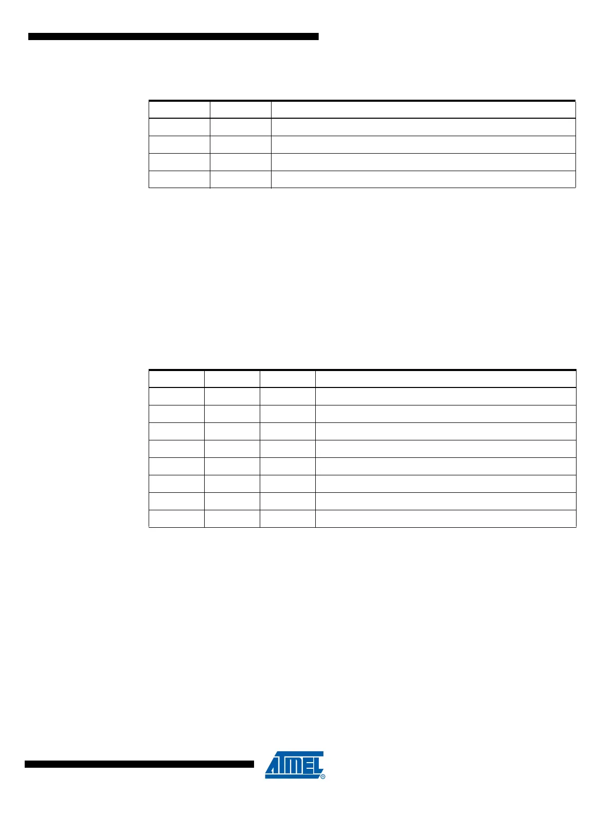
Table 18-12. Amplifier 2 Gain Selection
AMP2G1 AMP2G0 Description
00Gain 5
01Gain 10
10Gain 20
11Gain 40
Table 18-13. AMP1 Clock Source Selection
AMP2TS2 AMP2TS1 AMP2TS0 Clock Source
0 0 0 ADC Clock/8
0 0 1 Timer/Counter0 Compare Match
0 1 0 Timer/Counter0 Overflow
0 1 1 Timer/Counter1 Compare Match B
1 0 0 Timer/Counter1 Overflow
1 0 1 PSC Module 0 Synchronization Signal (PSS0)
1 1 0 PSC Module 1 Synchronization Signal (PSS1)
1 1 1 PSC Module 2 Synchronization Signal (PSS2)

 Loading...


