74
7647H–AVR–03/12
Atmel ATmega16/32/64/M1/C1
SS_A: Slave Port Select input. When the SPI is enabled as a slave, this pin is configured as an
input regardless of the setting of DDD0. As a slave, the SPI is activated when this pin is driven
low. When the SPI is enabled as a master, the data direction of this pin is controlled by DDD0.
When the pin is forced to be an input, the pull-up can still be controlled by the PORTD0 bit.
PCINT9, Pin Change Interrupt 9.
• PCINT8/PSCOUT1A/INT3
– Bit 0
PSCOUT1A, Output 1A of PSC.
INT3, External Interrupt source 3: This pin can serve as an external interrupt source to the MCU.
PCINT8, Pin Change Interrupt 8.
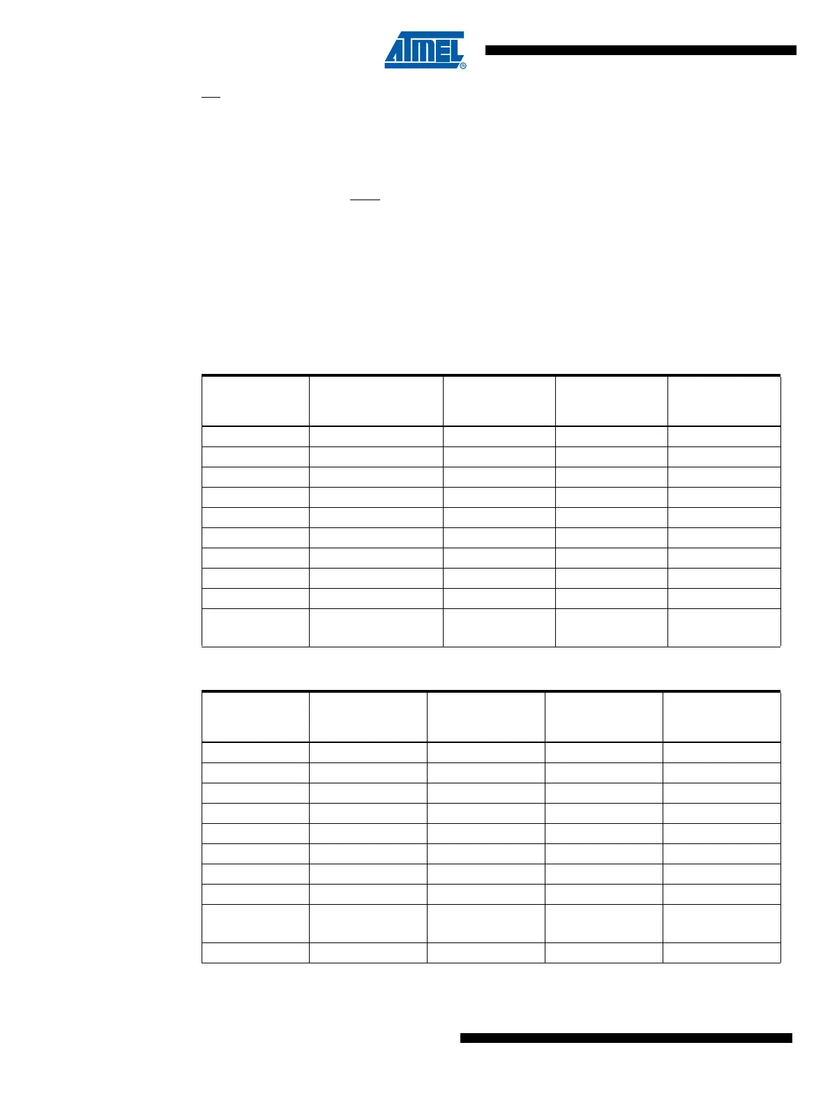
Table 9-7 and Table 9-8 relate the alternate functions of Port C to the overriding signals shown
in Figure 9-5 on page 67.
Table 9-7. Overriding Signals for Alternate Functions in PC7..PC4
Signal Name
PC7/D2A/AMP2+/
PCINT15
PC6/ADC10/
ACMP1/
PCINT14
PC5/ADC9/
AMP1+/ACMP3/
PCINT13
PC4/ADC8/
AMP1-/ACMPN3/
PCINT12
PUOE 0 0 0
PUOV 0 0 0
DDOE DAEN 0 0 0
DDOV 0 0 0 0
PVOE 0 0 0 –
PVOV 0 0 0 –
DIEOE DAEN ADC10D ADC9D ADC8D
DIEOV 0 0 0 0
DI
AIO – ADC10 Amp1 ADC9 Amp1+
ADC8 Amp1-
ACMPN3
Table 9-8. Overriding Signals for Alternate Functions in PC3..PC0
Signal Name
PC3/T1/RXCAN/
ICP1B/PCINT11
PC2/T0/TXCAN/
PCINT10
PC1/PSCIN1/
OC1B/SS_A/
PCINT9
PC0/INT3/
PSCOUT1A/
PCINT8
PUOE0000
PUOV0000
DDOE 0 PSCen10
DDOV1101
PVOE OC1Ben PSCen10
PVOV OC1B PSCout10
DIEOE In3en
DIEOV In3en
DI T1 T0
PSCin1
SS_A
INT3
AIO