Technical Data
Instruction handbook b maXX BM5500, BM5600, BM5700
Document No.: 5.13008.10
69
of 314
3
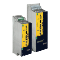
m With charging resistor BM553X-XR/BM553X-XS/BM553X-XW
BM5534 BM5535
Rated input power
1)2)
38 kVA 62 kVA
Rated input current
1)2)
(I
eff
) 55.0 A 89.0 A
Total harmonic distortion input current (THD
I
)
1)2)
107 %
14)
112 %
14)
Max. input current
2)
(I
eff
) 99.0 A 162.0 A
Rated DC link voltage
1)
(U
DC
) 540 V
DC
15)
DC link capacitance (internal) 1640 F 2000 F
DC link discharging time (internal DC link capacitance) 280 s 340 s
Waiting period between two switching-on operations
(no external DC link capacitance)
95 s 115 s
Max. permitted DC link capacitance (internal + external) 10810 µF
Waiting period between two switching-on operations
(with max. permitted DC link capacitance)
600 s
13)
Output voltage
1)3)
(U
AC
) 3 x 0 V to 3 x 370 V
Output frequency at 4 kHz
10)
0 Hz to 450 Hz
Rated output current
1)5)6)7)12)
(I
AC
) at 4 kHz
4)
45,0 A 60.0 A
Rated output current
1)5)6)7)12)
(I
AC
) at 8 kHz
4)
36,0 A 48.0 A
Output peak current
1)5)6)8)12)
(I
AC
) at 4 kHz
4)
90,0 A
Output peak current
1)5)6)8)12)
(I
AC
) at 8 kHz
4)
72,0 A
Max. peak current period
8)
60 s
Power supply DC link terminals Max. 10,0 kW
Brake resistor current, permitted (Î)
Max. 50.0 A
Brake resistor, external 16
Brake resistor threshold (Û) 780 V
Brake resistor peak power 40 kW
Permitted continuous brake r
esistor power external 10 kW
Power loss referring
to power input 600 W 840 W
Power input referring t
o control voltage 58 W
Current of the integrated brake control Max. 8.0 A
11)