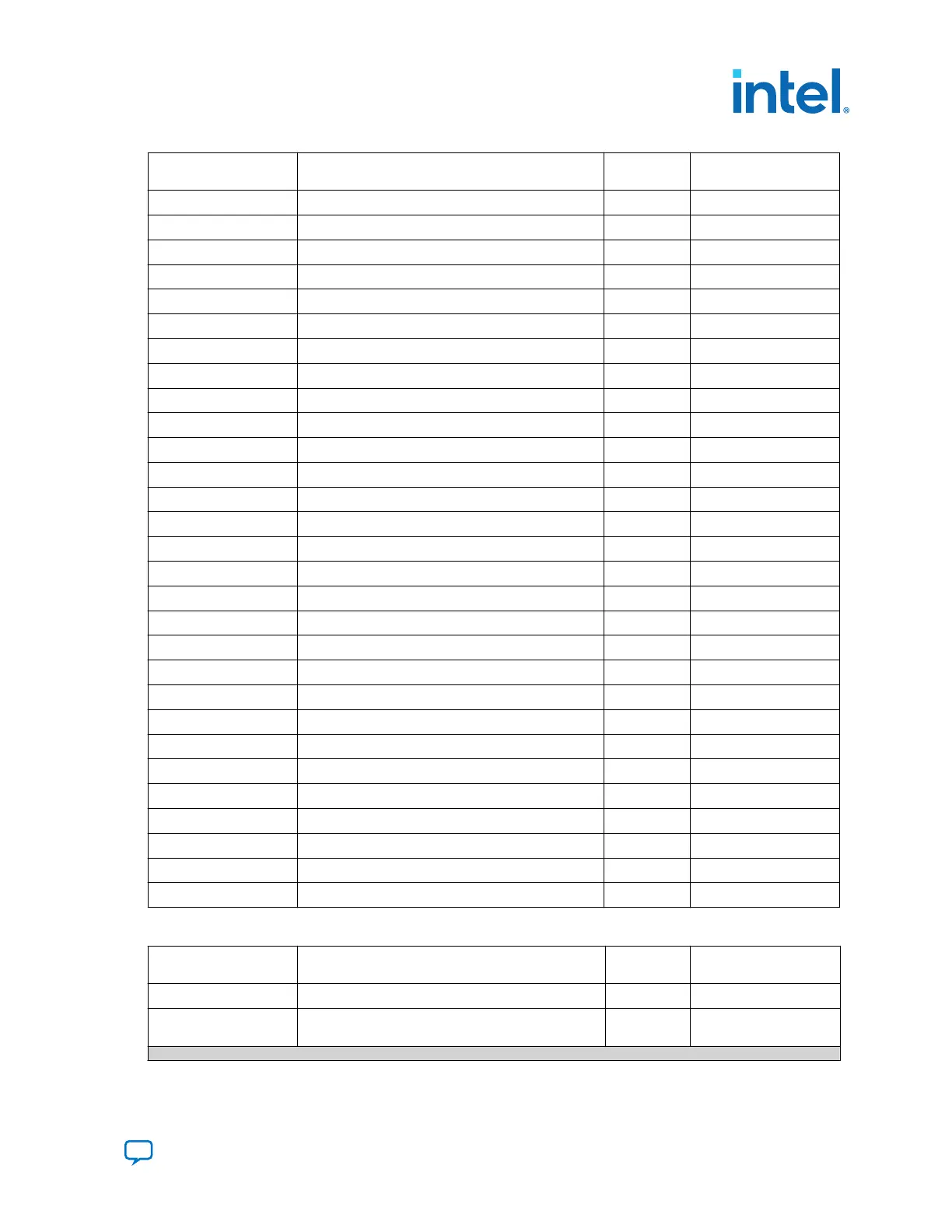
Board Reference Schematic Signal Name FPGA Pin
Number
I/O Standard
D27 FMCA_LA_TX_N13 AT20 LVDS
H32 FMCA_LA_TX_N14 AW16 LVDS
H35 FMCA_LA_TX_N15 BD18 LVDS
H38 FMCA_LA_TX_N16 AU20 LVDS
H7 FMCA_LA_TX_P0 AR22 LVDS
H10 FMCA_LA_TX_P1 AN20 LVDS
D11 FMCA_LA_TX_P2 AV11 LVDS
H13 FMCA_LA_TX_P3 AT17 LVDS
D14 FMCA_LA_TX_P4 AW13 LVDS
H16 FMCA_LA_TX_P5 AT14 LVDS
D17 FMCA_LA_TX_P6 AR17 LVDS
H19 FMCA_LA_TX_P7 AR9 LVDS
D20 FMCA_LA_TX_P8 AV19 LVDS
H22 FMCA_LA_TX_P9 AU11 LVDS
H25 FMCA_LA_TX_P10 AY10 LVDS
D23 FMCA_LA_TX_P11 AU18 LVDS
H28 FMCA_LA_TX_P12 BB15 LVDS
D26 FMCA_LA_TX_P13 AT19 LVDS
H31 FMCA_LA_TX_P14 AY16 LVDS
H34 FMCA_LA_TX_P15 BC18 LVDS
H37 FMCA_LA_TX_P16 AV20 LVDS
F1 FMCA_M2C_PG —
H2 FMCA_PRSNTN P16 1.8 V
C30 FMCA_SCL AU10 1.8 V
C31 FMCA_SDA AV10 1.8 V
J39 VIO_B_M2C — —
K40 VIO_B_M2C — —
K1 VREF_B_M2C — —
H1 VREF_FMCA — —
Table 34. FMC B Connector Pin Assignments, Schematic Signal Names
FMCB Connector Pin
Number
Schematic Signal Name FPGA Pin
Number
I/O Standard
D1 FMCB_C2M_PG — —
H5 FMCB_CLK_M2C_N0 K12 High Speed Differential
I/O
continued...
6. Board Components
683526 | 2023.07.12
Send Feedback
Intel
®
Arria
®
10 FPGA Development Kit User Guide
91

 Loading...


