Intel
®
Entry Server Chassis SC5299-E TPS Power Sub-system
Revision 3.1
Intel order number D37594-005
77
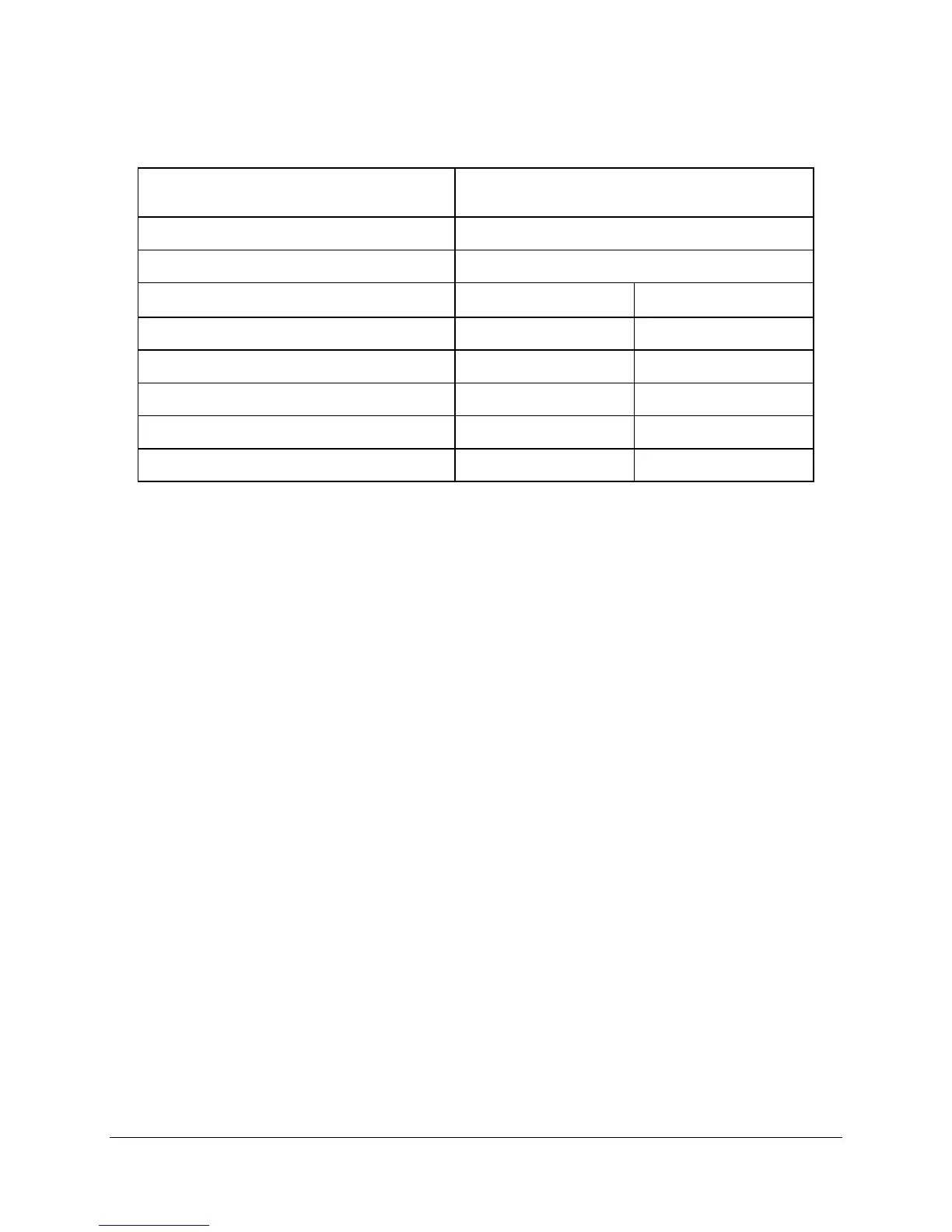
Table 93. PSON
#
Signal Characteristics
Signal Type
Accepts an open collector/drain input from the system.
Pull-up to VSB located in power supply.
PSON
#
= Low ON
PSON
#
= High or Open OFF
MIN MAX
Logic level low (power supply ON) 0V 1.0V
Logic level high (power supply OFF) 2.0V 5.25V
Source current, Vpson = low 4mA
Power up delay: T
pson_on_delay
5msec 400msec
PWOK delay: T
pson_pwok
50msec
2.4.5.2 PSKILL
The purpose of the PSKill pin is to allow for hot swapping of the power supply. The mating pin of
this signal on the cage input connector is tied to ground, and its resistance is less than 5 ohms.
2.4.5.3 PWOK (Power OK) Input and Output Signals
PWOK is a power OK signal and will be pulled HIGH by the power supply to indicate that all the
outputs are within the regulation limits of the power supply. When any output voltage falls below
regulation limits, or when AC power has been removed for a time sufficiently long so that power
supply operation is no longer guaranteed, PWOK will be de-asserted to a LOW state. The start
of the PWOK delay time is inhibited as long as any power supply output is within current limit.