7 APPLICATION INSTRUCTIONS
7.8 Buffer Memory Access Instructions
511
7
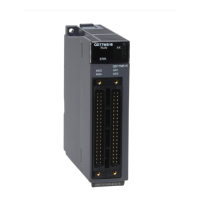
• The following program sets "A/D conversion disabled" to the CH1 and CH2 of the Q68ADV at I/O numbers 040 to 04F when
X0 is turned on (writes "3" to the buffer memory address 0).
• The following program zeroes the positioning address/movement amount of axis 1 of the QD75P4 at I/O numbers 040 to
05F when X0 is turned on (writes 0 to the buffer memory addresses 2006 and 2007).
• The value of n1 is specified by the upper 3 digits of hexadecimal 4 digits which represent the head I/O
number of an intelligent function module.
[QCPU]
[LCPU]
[Ladder Mode] [List Mode]
[Ladder Mode] [List Mode]
Step
Instruction
Device
Step
Instruction
Device
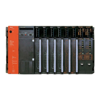
Power
supply
module
CPU QX10 QX10QX10 QX10
Q68
ADV
QY41
P
QY10 QY10
0000
H 0010H 0020H 0030H 0040H 0050H 0070H 0080H
Specify K4 or H4 as the head I/O number to be written.
Head I/O number configured in
the I/O assignment setting
Power
supply
module
CPU Built-in
I/0
Built-in
CC-Link
LX40
C6
LX40
C6
LX40
C6
L60
AD4
LY41
NT1P
LY10
R2
LY10
R2
LY10
R2
0000
H 0010H 0030H 0040H 0050H 0060H 0070H 0090H 00A0H 00B0H
CPU module
(L26CPU-BT)
Specify K6 or H6 as the head I/O number to be written.
Head I/O number configured in
the I/O assignment setting
 Loading...