Using the DF51
10/05 AWB8230-1541GB
50
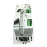
Block diagram
The following block diagram shows all terminals of the DF51.
OI Analog input, 4 to 20 mA
AM Analog output, 0 to 10 V
K11 Signalling relay terminal
K12 Signalling relay terminal (NC)
K14 Signalling relay terminal (NO)
CM2 Reference potential, transistor output
12 Transistor output, max. 27 V
11 Transistor output, max. 27 V
RJ 45 Interface connection for expansion
1 Digital input
2 Digital input
3 Digital input
4 Digital input
5 Digital input
L Common 0 V reference potential
H Reference voltage output, +10 V
O Analog input, 0 to +10 V
Figure 50: Block diagram, DF51
Power terminals
L, L1, L2, L3, NSupply (mains) voltage
U, V, W Frequency inverter output
L+, DC+ External DC choke
DC+, DC– Internal DC link
e, PE Positive earth
Control signal terminals
P24 Control voltage output, +24 V
5L
i
*
0 V
+10 V
0 V
PEWVU
M
3 ~
K11K12 K14
e
AM H O OI L
CM2
12 11
0...10 V
RUN
FA1
4...20 mA
0...10 V
–
+
–
+
L+
DC–
DC+
PEL3L2L1
3
1
PEN
L
FF2
FF1
REV
FWD
3214
P24
+24 V
RJ 45
ModBus
RST
* PNU C005 = 19 (PTC)