5.4.3 READ SWITCH
The diode switch CR46,
CR51
(zone
F10,
11), CR48 and
CR52
(zone
E10,
11) is used to
isolate the head bus from the read amplifier during Write operations to prevent overload
of
the read preamplifier.
During a Write operation,
Q8
(zone H14) is turned on via open-collector driver U12-D. This
pulls the
junction
of
R83
and
R84
(zone
E11)
to
+10v
cutting
off
all four diodes. This
follows
si nce the head bus voltage cannot exceed + 10v and the anode voltage
of
CR51
and
CR52
cannot exceed +
O.
7v
due to
CR55
and CR56.
During a Read operation,
Q8
is turned
off
and the
junction
of
R83
and
R86
is returned to
approximately
-6v
via
R85.
Thus, approximately 1 ma
flows
through
R83
(and
R84)
and
approximately
0.5 ma is supplied
by
R88
(and R86). Thus, a current
of
0.5 ma
flows
through each
of
the diodes CR46,
CR51
, CR48, and CR52 enabling the read switch.
5.4.4 READ PREAMPLIFIER
The balanced read signal from the head bus is terminated by
R89
or L7,
C11
and
R90
or L8,
C12
(zone
E10)
and fed to the type
733
differential video
amplifier
U1. When used
in
this
configuration the amplifier has a wide bandwidth and a balanced-to-single-ended
output
gain
of
approximately
50
for
100 tpi
or
150
for
200
tpi.
5.4.5
FILTER
The single-ended preamplifier
output
of
video amplifier
U1
is fed via matching resistor
R100
to a I inear phase filter. This filter has sharp
cut-off
characteristics combined with a
group delay characteristic which is constant over the signal frequency band. The insertion
loss
of
this
filter
is 0.5.
5.4.6 VARIABLE GAIN AMPLIFIER
The Variable Gain
Amplifier
consists
of
transistor
amplifier
Q27
(zone
E8)
employing
emitter feedback
to
control its gain. It can be seen that the
emitter
resistance
of
this
amplifier can
be
one of
two
values:
680
ohms (R106) when
Q26
is not conducting, and
220
ohms (R106 in parallel with
R104)
when
Q26
is conducting. Normally,
Q26
is conducting
and the gain
of
the stage is approximately
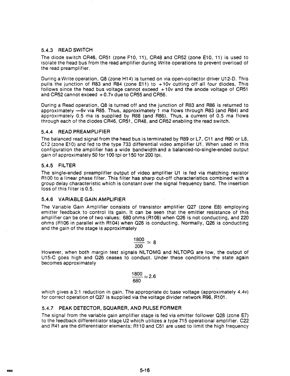
1800
~
8
200
However, when both margin test Signals NLTOMG and NLTOPG are low, the
output
of
U15-C goes high and
Q26
ceases to conduct. Under these
conditions
the state again
becomes approximately
1800
~
2.6
680
which gives a
3:1
reduction in gain. The appropriate de base voltage (approximately 4.4v)
for correct operation
of
Q27
is supplied via the voltage divider network
R96,
R101
.
5.4.7 PEAK DETECTOR,
SQUARER, AND PULSE FORMER
The
Signal from the variable gain amplifier stage is fed via
emitter
follower
Q28
(zone
E7)
to the feedback differentiator stage
U2
which utilizes a type
715
operational amplifier.
C22
and
R41
are the differentiator elements;
R110
and
C51
are used
to
limit
the high frequency
5-16
 Loading...