5.7
TEMPERATURE
COMPENSATION
PCBA
The
Temperature Compensation
PCBA
is installed in
200
tpi 03000 Disk Drives.
The
PCBA
is located adjacent to the Read/Write
PCBA
and is approximately
203.2
mm
(8
inches)
long
by
101.6
mm
(4
inches) high.
The
Temperature Compensation
PCBA
operates in
conjunction with one externally mounted termistor to provide
thermal compensation to
200
tpi models. Refer to Schematic No.
103976
(sheet 3 only) and Assembly No.
103977.
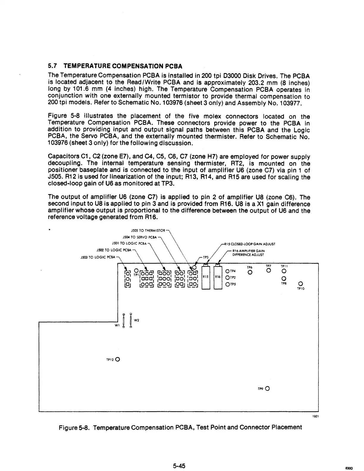
Figure
5-8
illustrates the placement of the five molex connectors located on the
Temperature Compensation
PCBA. These connectors provide power to the
PCBA
in
addition to providing input
and
output signal paths between this
PCBA
and the Logic
PCBA,
the Servo
PCBA,
and
the externally mounted thermister. Refer to Schematic No.
103976
(sheet 3 only) for the following discussion.
Capacitors
C1
,
C2
(zone
E7),
and
C4,
C5,
ca,
C7
(zone
H7)
are
employed for power supply
decoupling.
The
internal temperature sensing thermister,
RT2,
is mounted
on
the
positioner baseplate
and
is connected to the input of amplifier
U6
(zone
C7)
via pin 1 of
J505.
R12
is used for linearization of the input;
R13, R14,
and
R15
are
used for scaling the
closed-loop gain of
U6
as
monitored at
TP3.
The
output of amplifier
U6
(zone
C7)
is applied to pin 2
of
amplifier
U8
(zone
C6).
The
second input to
U8
is applied to pin 3
and
is provided from
R16.
U8
is a
X1
gain difference
amplifier whose output is proportional to the difference between the output of
U6
and
the
reference voltage generated from
R16.
TPI20
15
ClOSED-LOOP
GAIN
ADJUST
Rib
AMPLIFIER
GAIN
DIFFERENCE
ADJUST
TP6
o
TP7
0
OTPS
mO
TPll
0
0
TP8
0
TP10
Figure 5-8. Temperature Compensation
PCBA,
Test Point
and
Connector Placement
1921
630D