LINE
LINE
CONNECT
VOLTAGE
BETWEEN
95
13
AND
3
12
TO
13
AND
3
TO
7
;00
6
AND
3
2
TO
6
AND
3
TO
7
110
5
AND
3
I
TO
5
AND
3
TO
7
l1S
6
AND
4
2
TO
6
AND
4
TO
a
125
5
AND
4 1
TO
5
AND
4
TO
8
:90
13
AND
3
12
TO
7
200
6
AND
3 2
TO
7
210
6 AND J
I
TO
7
215
6
AND
~
2
TO
7
220
5
AND
3 I
TO
7
225
5
AND
4
2
TO
7
230
6
AND
4 2
TO
8
235
5 AND 4 1
TO
7
2~
6 AND 4
I
TO
8
250
5 AND
~
I
TO
a
NOTE,
THIS
TABLE
APPLIES
TO
POWER
SUPPLY
ASSEMBLY
NUMBER
1027~I-01
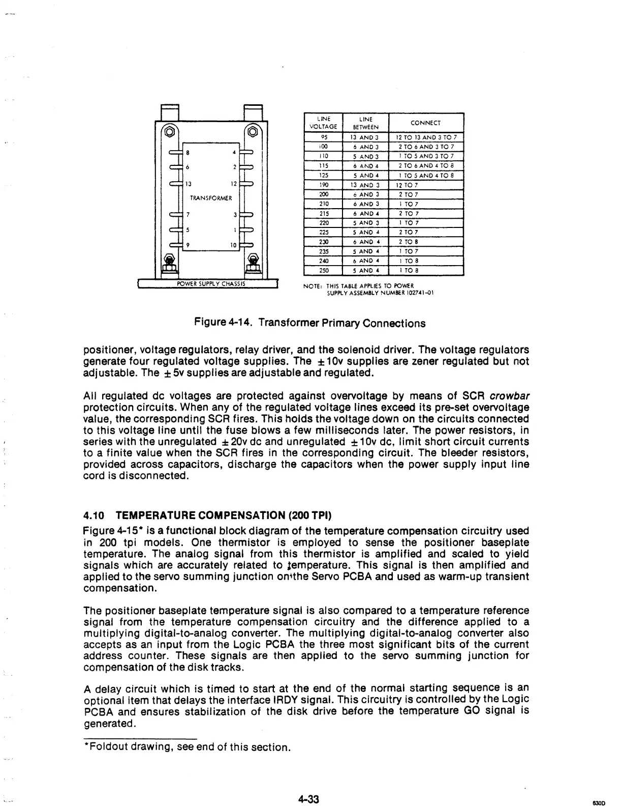
Figure 4-14. Transformer Primary Connections
positioner, voltage regulators, relay driver, and the solenoid driver. The voltage regulators
generate four regulated voltage
supplies. The ± 10v supplies are zener regulated but not
adjustable. The
±
Sv
supplies are adjustable and regulated.
All regulated dc voltages are protected against overvoltage by means
of
SCR
crowbar
protection circuits. When any
of
the regulated voltage lines exceed its pre-set overvoltage
value, the corresponding
SeR fires. This holds the voltage down on the circuits connected
to this voltage
line until the fuse blows a few milliseconds later. The power resistors, in
series with the unregulated
±
20v
dc and unregulated ± 1
Ov
dc,
limit
short
circuit
currents
to a finite
value when the
SCR
fires in the corresponding circuit. The bleeder resistors,
provided across capacitors, discharge the capacitors when the power supply input
line
cord is disconnected.
4.10 TEMPERATURE COMPENSATION (200 TPI)
Figure 4-1S* is a functional block diagram
of
the temperature compensation circuitry used
in
200
tpi models. One thermistor is employed to sense the positioner baseplate
temperature. The analog signal from this thermistor is amplified and scaled to
yield
signals which are accurately related to temperature. This signal is then amplified and
applied to the servo summing junction
on
1
the Servo PCBA and used as warm-up transient
compensation.
The positioner baseplate temperature
Signal is also compared
to
a temperature reference
Signal from the temperature compensation circuitry and the difference applied to a
multiplying digital-to-analog converter. The multiplying digital-to-analog converter
also
accepts as
an
input from the Logic PCBA the three most significant
bits
of
the current
address counter. These Signals are then applied to the servo summing
junction
for
compensation
of
the
disk
tracks.
A
delay circuit which is timed to start at the end
of
the normal starting sequence is
an
optional item that delays the interface
IRDY
signal. This circuitry is controlled by the LogiC
PCBA and ensures stabil ization
of
the disk drive before the temperature
GO
signal is
generated.
*Foldout drawing,
see
end
of
this section.
4-33
6300