6.12.3 DATA AND CLOCK PULSEWIDTH
6.12.3.1 Test Configuration
(1)
Remove the interface connector and terminator PCBA from connector
J101
and
J1
02
on the Logic PCBA.
(2)
Connect a disk exerciser having read/write capability
to
J101
or J102 on the Logic
PCBA.
(3)
Apply power to the exerciser and the disk drive. Observe that the READY indicator
is illuminated;
allow a 5-minute warm
up
period.
(4)
Write
an
all-ones pattern via the disk exerciser.
(5)
Connect oscilloscope Channel 1 probe to
TP25.
Connect the test probe ground
clip to ground reference
TP17.
(6)
Set oscilloscope Channel 1 sensitivity
to
0.1
Ov
per division.
(7)
Set sync
to
internal, normal mode.
(8)
Set oscilloscope
to
trigger on the positive slope of RPN.
(9)
Connect oscilloscope Channel 2 probe
to
read
data
TP15
(or
read
clock TP16).
Connect the test probe ground clip
to
ground reference TP17.
(10)
Position sweep trace 1.3 cm below cener line of graticule.
(11)
Set oscilloscope Channel 2 sensitivity
to
0.10v per division.
6.12.3.2 Test Procedure
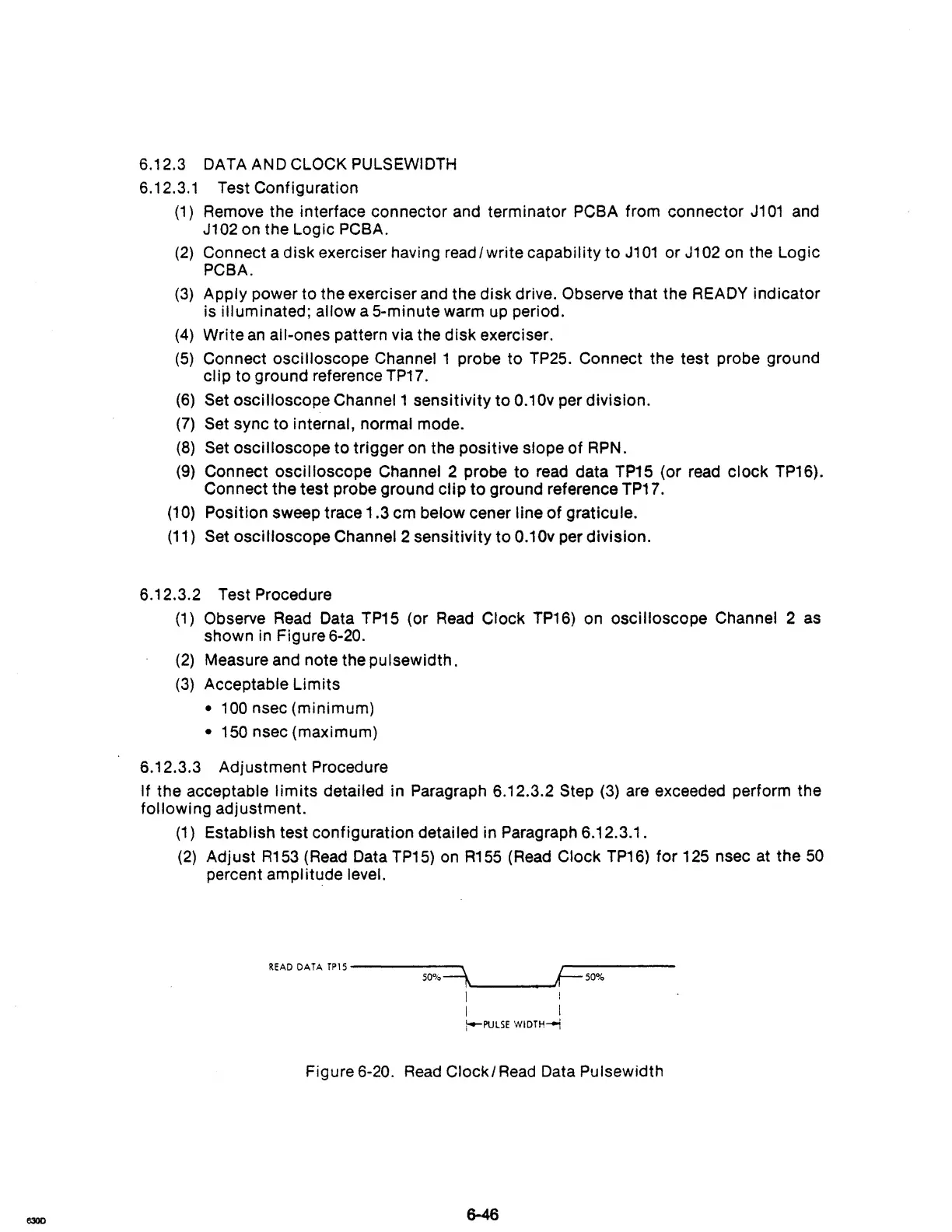
(1)
Observe
Read
Data
TP15
(or
Read
Clock
TP16)
on oscilloscope Channel 2
as
shown
in
Figure 6-20.
(2)
Measure and note the pulsewidth.
(3)
Acceptable Limits
•
100
nsec (minimum)
• 150 nsec (maximum)
6.12.3.3 Adjustment Procedure
If the acceptable
limits
detailed in Paragraph 6.12.3.2 Step
(3)
are exceeded perform the
following adjustment.
(1)
Establish test configuration detailed in Paragraph 6.12.3.1.
(2)
Adjust
R153
(Read Data
TP15)
on
R155
(Read Clock
TP16)
for
125 nsec at the
50
percent amplitude level.
READ
DATA
TP15
-----~
~-----
50"10-1,
It-
50%
I I
I I
!-PUlSE
WIDTH"'"
Figure 6-20.
Read
Clockl
Read
Data Pulsewidth