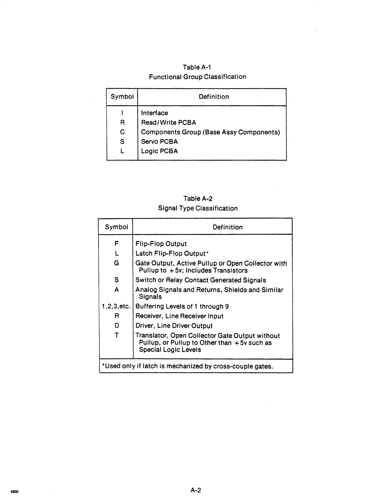
Table
A-1
Functional Group Classification
Symbol
Definition
I Interface
R Read/Write PCBA
C
Components Group (Base Assy Components)
S
Servo
PCBA
L Logic PCBA
TableA-2
Signal Type Classification
Symbol
Definition
F
Flip-Flop Output
L Latch Flip-Flop Output*
G
Gate Output, Active
Pullup or
Open
Collector with
Pullup to +
5v;
Includes Transistors
S Switch
or
Relay Contact Generated Signals
A
Analog Signals and Returns, Shields and Similar
Signals
1,2,3,etc. Buffering Levels of 1 through 9
R
Receiver, Line Receiver
Input
D
Driver, Line Driver
Output
T
Translator,
Open
Collector Gate Output without
Pullup,
or
Pullup to Other than +
5v
such
as
Special Logic Levels
*Used only
if
latch is mechanized by cross-couple gates.
A-2