RH850/F1Kx, RH850/F1K Series Hardware Design Guide
R01AN3841ED0110 Rev. 1.10 Page 101 of 108
August 8, 2019
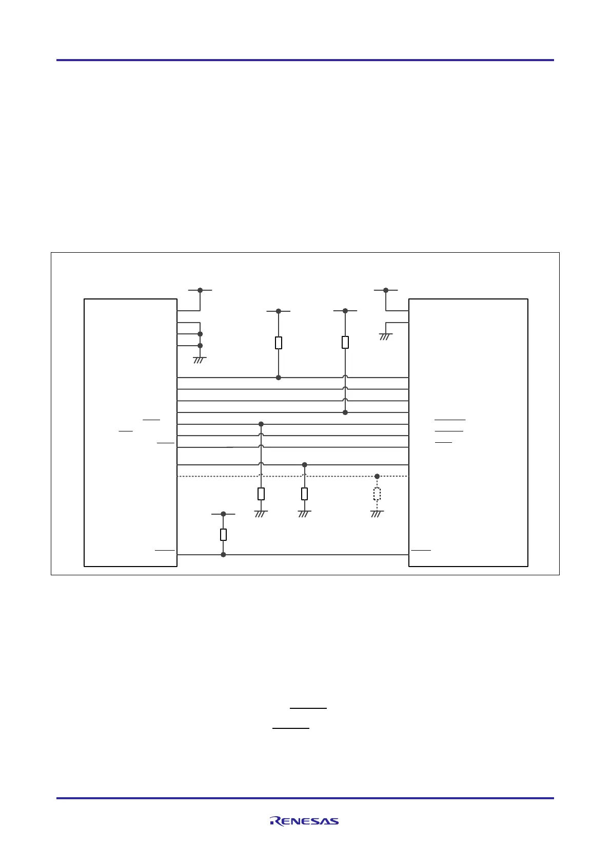
8.3 Combined Debug and Flash Programming Interface Connection
The following figure describes the combined connections for debugging and flash programming, supporting
• Low pin debug interface (1 pin) - hereinafter called "LPD (1 pin)"
• Low pin debug interface (4 pins) - hereinafter called "LPD (4 pins)"
• Nexus interface
• Single-wire asynchronous flash programming interface with PG-FPx or E1/E2 & RFP
• Two-wire asynchronous flash programming interface with PG-FPx or E1/E2 & RFP
• Synchronous flash programming interface with PG-FPx
Figure 43: Combined debug and flash programming interface connections
The use of an external resistor is only required when the Nexus IF mode is used for debugging
and depends on the hardware specification and implementation of the 3
rd
party development
tool.
When the Nexus interface is used for debugging the value of the resistor depends on the 3
rd
party development tool specification.
The resistor is optional when the LPD (4 pins) mode is used
The maximum sink current of the RESET terminal of the E1/E2 emulator is 2mA. The
external pull-up circuit of the
RESET pin has to be considered based on the applications
requirement. When an external RESET component is used, the pull-up resistor value has to be
selected appropriately.
TVDD
GND
GND
GND
VDDVDD
EVCC
EVSS
FPDR/TDI/LPDIO/TxD/SO
FPDT/TDO/LPDO/SI
TCK/LPDCLK/SCK
TMS
TRST/CLK
RDY /LPDCLKOUT
FPM D0
FPM D1
RESET
RESET
P10_8 ( FLMD1)
No te 5
FLM D0
JP0_0 (DCUTDI/LPDIO, LPDI)
JP 0_ 1 ( DCUTDO/LPDO)
JP0_2 (DCUTCK/LPDCLK)
JP0_3 (DCUTMS)
JP0_4 (DCUTRST)
JP 0_ 5 ( DCURDY/LPDCLKOUT)
VDD
1k to 10kΩ
No te 3
RH85 0/F1Kx, RH85 0/F1 K
Emulator /
PG-FPx Flash Programmer
(14pin Connector)
Mi n.
86kΩ
1k to 10kΩ
RDY /LPDCLKOUT
EVTO JP0_6 ( EVTO)
VDD
No te 1
10k to 100 kΩ
No te 2
VDD
min. 4.7kΩ
No te 4

 Loading...


