RH850/F1Kx, RH850/F1K Series Hardware Design Guide
R01AN3841ED0110 Rev. 1.10 Page 99 of 108
August 8, 2019
Design the circuit in the way that the FLMD1 pin must be at the low level during serial
programming. During programming, it outputs a low level on FPMD1 to place the device in the
serial programming mode.
If necessary, connect FPMD1 and FLMD1.
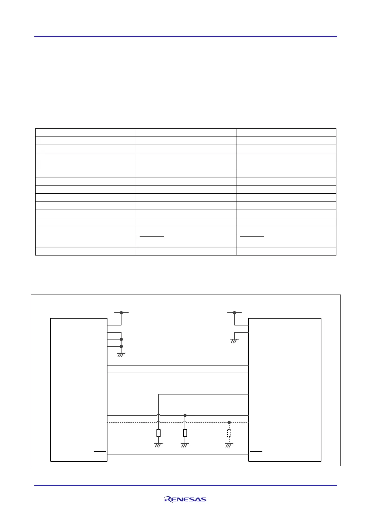
The flash programming signal connection of the PG-FPx interface is given in the table below:
Table 72: PG-FPx Flash programming signal connection
PG-FPx Interface Connector
13 RESET RESET
8.2.2 Flash Programming by E1/E2 Emulator and RFP
Figure 42: E1/E2 flash programming interface connection
TVDD
GND
GND
GND
VDDVDD
EVCC
EVSS
FPDR
FPDT
FPM D0
FPM D1
RESET RESET
P10_8 (FLM D1)
No te
FLM D0
JP0_0 (RxD/TxD)
JP0_1 (TxD)
RH850/F1Kx, RH850/F1K
E1/E2 & RFP Flash
Programmer
(14pin Connector)
Min.
86kΩ
1k t o 10kΩ
JP0_4
10k to 100kΩ

 Loading...


