EasyManuals Logo

Renesas RH850/F1Kx Series Hardware Design Guide

Renesas RH850/F1Kx Series
112 pages
To Next Page IconTo Next Page
To Previous Page IconTo Previous Page
Page #97 background imageLoading...
Page #97 background image
RH850/F1Kx, RH850/F1K Series Hardware Design Guide
R01AN3841ED0110 Rev. 1.10 Page 97 of 108
August 8, 2019
When the Nexus debug mode is used, the ports of the JP0 port group are automatically switched to the debug interface
mode.
JP0_0: DCUTDI input
JP0_1: DCUTDO output
JP0_2: DCUTCK input
JP0_3: DCUTMS input
JP0_4:
DCUTRST input
JP0_5: DCURDY
output
JP0_6: EVTO
(depending on device)
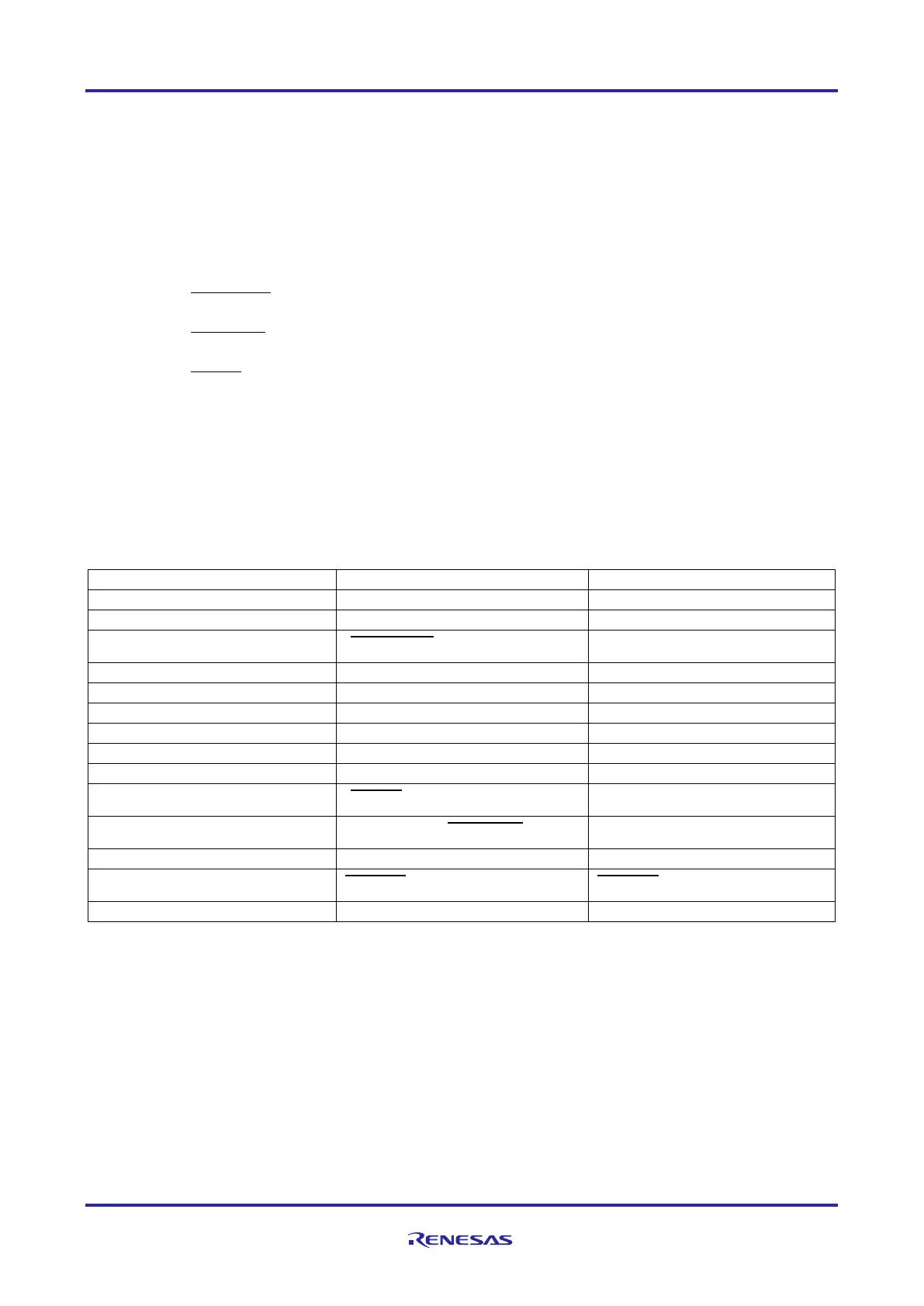
The debug interface signal connection of the E1/E2 interface is given in the table below:
Table 70: Debug interface signal connection
E1/E2 Interface Connector
E1/E2 Interface Signal
Device Pin
1
LPDCLK/(DCUTCK)
JP0_2
2
GND
EVSS
3 ( DCUTRST ) JP0_4
4
FPMD0/FLMD0
FLMD0
5
LPDO/(DCUTDO)
JP0_1
6
FPMD1
FLMD1
7
LPDI/LPDIO/(DCUTDI)
JP0_0
8
TVDD
EVCC
9
(DCUTMS)
JP0_3
10 ( EVTO ) JP0_6
Note 2
11 LPDCLKOUT/( DCURDY ) JP0_5
12
GND
EVSS
13
RESET
RESET
14
GND
EVSS
Notes:
1.
The Nexus interface signals marked with (text) are supported by 3rd party development tools
and not by E1/E2 emulator.
2.
Depending on the device.

Table of Contents

Other manuals for Renesas RH850/F1Kx Series

Questions and Answers:

Question and Answer IconNeed help?

Do you have a question about the Renesas RH850/F1Kx Series and is the answer not in the manual?

Renesas RH850/F1Kx Series Specifications

General IconGeneral
BrandRenesas
ModelRH850/F1Kx Series
CategoryComputer Hardware
LanguageEnglish

Related product manuals