RH850/F1Kx, RH850/F1K Series Hardware Design Guide
R01AN3841ED0110 Rev. 1.10 Page 104 of 108
August 8, 2019
9. Test Tool Interface
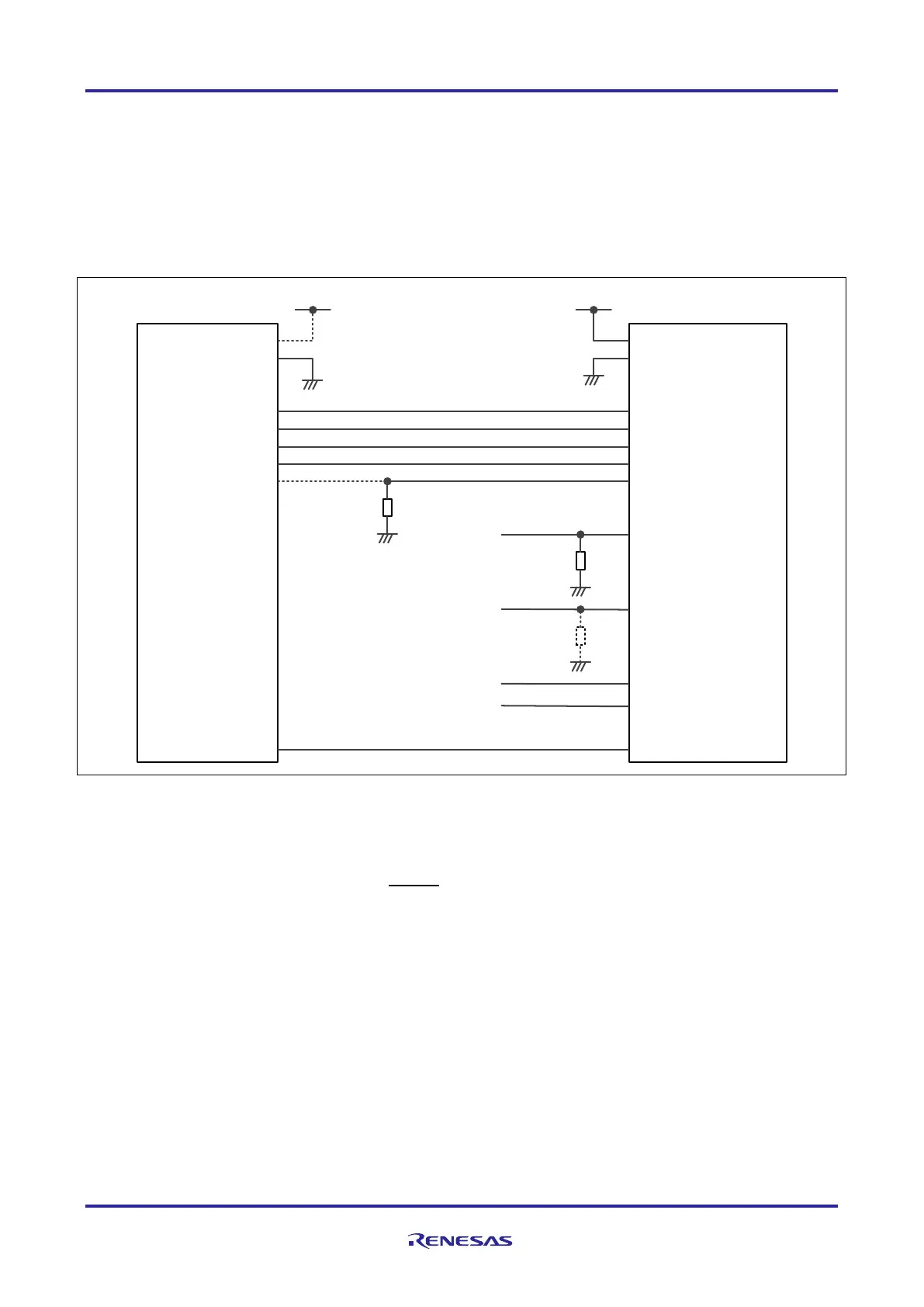
The boundary scan test is compliant with IEEE Standard 1149.1 and certain boundary scan instructions are supported.
When the boundary scan mode shall be used, several connections have to be done between boundary scan test tool and
the device. Especially the boundary scan mode selection pins have to be considered from application point of view as
these pins are normally used for application related functions.
Figure 45: Boundary scan connection of RH850/F1Kx and RH850/F1K series
During boundary scan mode the level of the following pins must be fixed: P10_1: Low, P10_2:
High, P10_8: High
2. The pin availability of JP0_6/ EVTO depends on the selected device.
In case of the digital I/O pins shared with an analog buffer the boundary scan function only applies to the general I/O
function:
• ADCA0: AP0, P8 and P9
• ADCA1: AP1, P18 and P19 (availability depending on the device)
VDD
GND
VDDVDD
EVCC
EVSS
TDI
TDO
TCK
TMS
TRST (optiona l)
RDY
RESET
RESET
P10_8 (FLM D1)
FLM D0
JP0_0 (DCUTDI)
JP0_1 (DCUTDO)
JP0_2 (DCUTCK)
JP0_3 (DCUTMS )
JP0_4 (DCUTRST)
JP0_5 (DCURDY )
RH850/F1Kx, RH850/F1K
Boundary Scan Test Tool
(Connector)
Min.
86kΩ
1k t o 10kΩ
P10_1 (MODE0)
P10_2 (MODE1)
Set to high-le vel
Set to high-le vel
Set to low-level
Set to high-le vel
(optiona l)
JP0_6 (EVTO)EVTO
10k to 100kΩ

 Loading...


