RH850/F1Kx, RH850/F1K Series Hardware Design Guide
R01AN3841ED0110 Rev. 1.10 Page 45 of 108
August 8, 2019
1.5.2 Power Supply Pin Configuration of RH850/F1K
The following shows power supply pin configuration. Do not open any power and GND terminals even if those are
internally connected.
• The EVCC supply pins are internally connected
• The EVSS pins are internally connected.
• AWOVSS and ISOVSS are internally connected.
• Others are not internally connected.
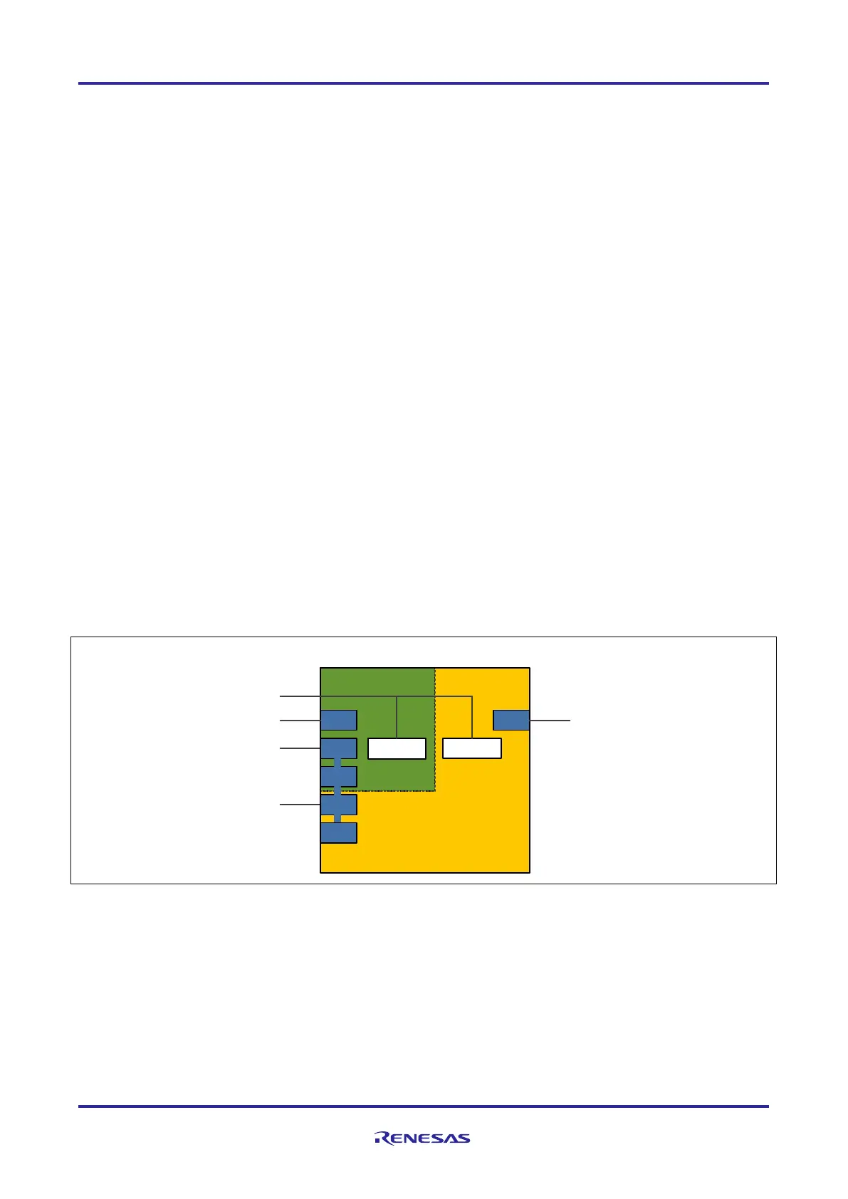
1.5.3 Power Supply Pin Architecture of RH850/F1K
The RH850/F1K supports different power supply architectures. The power supply architecture depends on the chosen
RH850/F1K device, application requirements and the use case.
Some common conditions apply to the supply of the RH850/F1K:
• REGVCC = EVCC = VPOC to 5.5V
• A0VREF = 3.0V to 5.5V
• A1VREF = 3.0V to 5.5V (when available on the device)
• AWOVSS = ISOVSS = EVSS = A0VSS = A1VSS = 0V
The following figure and the different cases describe the impact to the ADC ports and the ports with analog/digital
function depending on the power supply architecture. In addition, it describes the limitations to these ports.
Figure 16: RH850/F1K Power supply architecture
Note: The A1VREF supply pin availability depends on the chosen device.
RH850/F1K
AWO-Are a ISO-Are a
AP0
REGVCC
A0VREF
EVCC
EVCC
Pn
Regulator
Regulator
P8
P9
Pm
AP1
A1VREF

 Loading...


