RH850/F1Kx, RH850/F1K Series Hardware Design Guide
R01AN3841ED0110 Rev. 1.10 Page 61 of 108
August 8, 2019
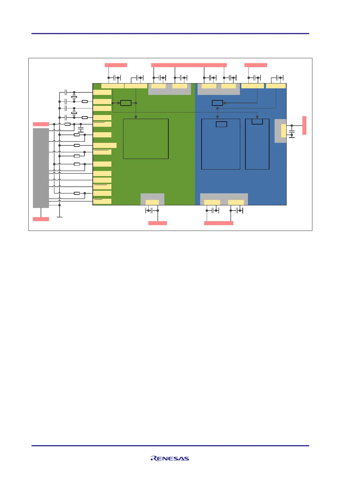
2.4 Minimum External Components of RH850/F1KH-D8
Figure 24: Minimum external components of RH850/F1KH-D8 in normal operating mode
Note: The debug interface connections shown covers Nexus, LPD (1 pin) and LPD (4 pins). For details of the single
debug connection, see Chapter 8, Development Tool Interface for the corresponding debug interface. For details
of other external components, see their related chapters.
Port
BVCC BVCC
ADCA1
AD1
Port
EVCC ISOVCL
Port
EVCCAWOVCL
ADCA0
AD0
A0VREF
C6
BVCC
C7 C8
C9
A1VREF
C12C13 C10C15
X1
X2
IP0_0
XT1
RESET
FLM D0
P10_8/FLMD1
DC U TRS T
DCU TDI
DCU TDO
D C U CL K
DCU RDY
DC U TMS
EVCC
C14
EVCC
De bug
VDD
REG
Logic
Logic Flash
REG
REG
C1
Q1
Q2
C2
C3
C4
R1
R2
R3
R4
R5
Cor e
C5
R6
EV TO
EVCC
R7
R8
EVCC
C11
REG0V CC
REG0V CC
C16
REG1V CC
REG1V CC
C17

 Loading...


