RH850/F1Kx, RH850/F1K Series Hardware Design Guide
R01AN3841ED0110 Rev. 1.10 Page 11 of 108
August 8, 2019
Table 5: RH850/F1KM-S1 Power supply architecture with mixed supply 5V & 3.3V
Case 3 and Case 4 – Mixed Supply 5V & 3.3V
EVCC = 3.3V or 5V
A0VREF = don’t care
Common condition REGVCC = EVCC not met
Table 6: RH850/F1KM-S1 Power supply architecture with mixed supply 5V & 3.3V
Case 5 – Mixed Supply 5V & 3.3V
EVCC = 3.3V
A0VREF = 5V
AP0 – Port usable with analog or digital function
P8 – Port usable with analog or digital function, analog input voltage
limited to max. 3.3V, reduced AD conversion range between 0V to 3.3V
P9 – Port usable with analog or digital function, analog input voltage
limited to max. 3.3V, reduced AD conversion range between 0V to 3.3V
Analog port function limitation applies to P8 and P9
Table 7: RH850/F1KM-S1 Power supply architecture with single supply 3.3V
Case 6 – Single Supply 3.3V
EVCC = 3.3V
A0VREF = 3.3V
AP0 – Port usable with analog or digital function
P8 – Port usable with analog or digital function
P9 – Port usable with analog or digital function
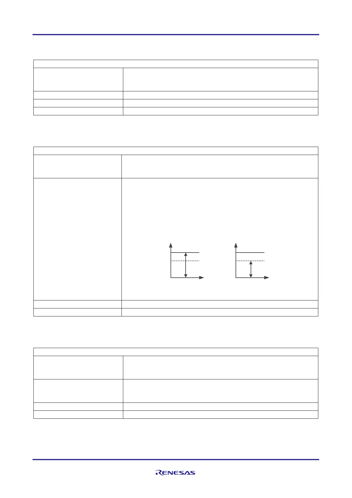
3FFh
0V
3.3V
5V
2A3h
0V
3.3V
5V
Note: Conversion range example based on 10-bit ADC resolution
Analog input channel on AP0
Analog input channel on P8, P9
Red uced AD c onversion range
Available
voltage range
Available
voltage range

 Loading...


