RH850/F1Kx, RH850/F1K Series Hardware Design Guide
R01AN3841ED0110 Rev. 1.10 Page 62 of 108
August 8, 2019
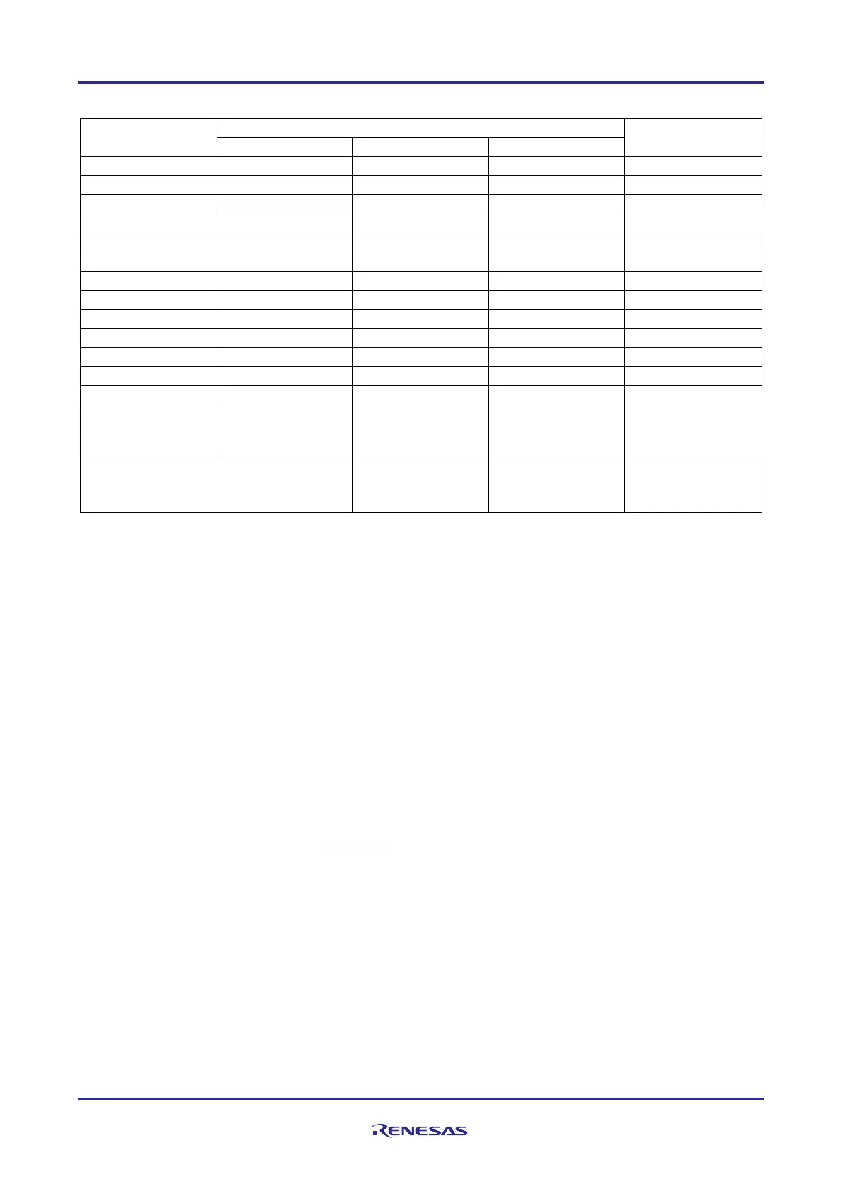
Table 56: Minimum external components for RH850/F1KH-D8 (324pin)
C11, C12, C13,
ESR: max. 40
[mΩ]
ESR: max. 40
[mΩ]
ESR: max. 40
[mΩ]
See Chapters 3.1.1, Main Oscillator and 3.1.2, Sub Oscillator for details.
The shown values are for reference only.
It must be ensured (by the schematic/PCB designer) that the voltage levels at the device pins always
remain within the specified range of the electrical characteristics (described in the RH850/F1Kx
hardware user’s manual).
See Chapter 4.2.1, Minimum RESET Circuit for details.
A low level must be applied to FLMD1 in case FLMD0 becomes ‘1’ for external flash programming.
As a minimum value, a direct connection to VSS can be applied. But in case the related port (P10_8) is
switched to output ‘1’, it will damage the port/device.
In case of smaller values than the min. value, the typically connected device (ex. E1 emulator) is not able
to apply a high (‘1’) signal.
See Chapters 8, Development Tool Interface and 9, Test Tool Interface for details.
See Chapters 4.3.2, JP0_4/ DCUTRST , 4.4.4, Recommended Connection of Unused Pins and 8,
Development Tool Interface for details.
The resistor is only required when the JTAG/Nexus interface is used for debugging and depends on the
specification of the 3
rd
party development tool specification. See Chapters 8, Development and 9, Test
Tool Interface for details.

 Loading...


