RH850/F1Kx, RH850/F1K Series Hardware Design Guide
R01AN3841ED0110 Rev. 1.10 Page 42 of 108
August 8, 2019
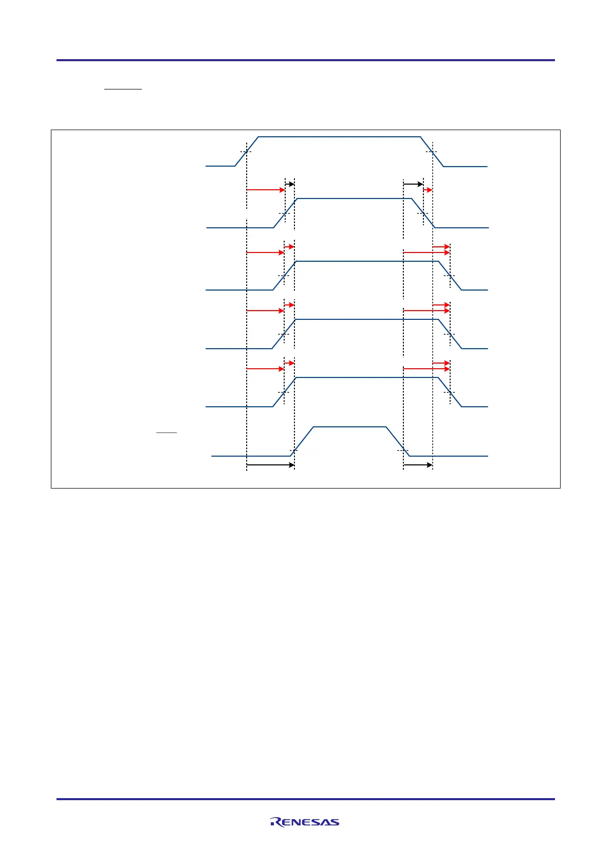
a) When
RESET terminal is used
Figure 14: RH850/F1KH-D8 Power up/down timing
Note 1. Both t
DPOR
timing should be kept.
Note 2. Both t
DRPD
timing should be kept.
Note 3. For the spec of t
DPOR
, t
DRPD
and t
VS
, please refer to Section 47A.4.5.3, Power Up/Down Timing of the
RH850/F1KH, RH850/F1KM Hardware User’s Manual.
REG
0VCC/ EVCC
VP OC( mi n)
BVCC
3.0V
0V
RESET
0V
0V
VIL
A0 VRE F
3.0V
0V
A1VREF
3.0V
0V
Min. 0 us
Max . 0.5/tVS ms
Min. 0 us
Min. 0 us
Min. 0 us
Min. 0 us
t
DP OR
No te 1
Max . 0.5/tVS ms
Min.
0 us
Max . 0.5/tVS ms
Min. 0 us
t
DRP D
No te 2
Min. 0 us
REG1VCC
VP OC( mi n)
0V
Min. 0 us
Min. 0us
t
DP OR
No te 1
Min. 0 us
t
DRP D
No te 2

 Loading...


