RH850/F1Kx, RH850/F1K Series Hardware Design Guide
R01AN3841ED0110 Rev. 1.10 Page 93 of 108
August 8, 2019
8. Development Tool Interface
The description of the development tool interface in this chapter assumes that the normal operating mode of the MCU is
used. When the user boot mode shall be used the configuration of the pins FLMD0, P10_8/FLMD1, P10_1/MODE0,
P10_2/MODE1 and P10_6/MODE2 has to be set accordingly.
8.1 Debug Interface Connection
For the debugging environment, the following interface connections are supported:
• Low pin debug interface (1 pin) - hereinafter called "LPD (1 pin)"
• Low pin debug interface (4 pins) - hereinafter called "LPD (4 pins)"
• Nexus interface
o The Nexus interface is only supported by 3rd party development tools.
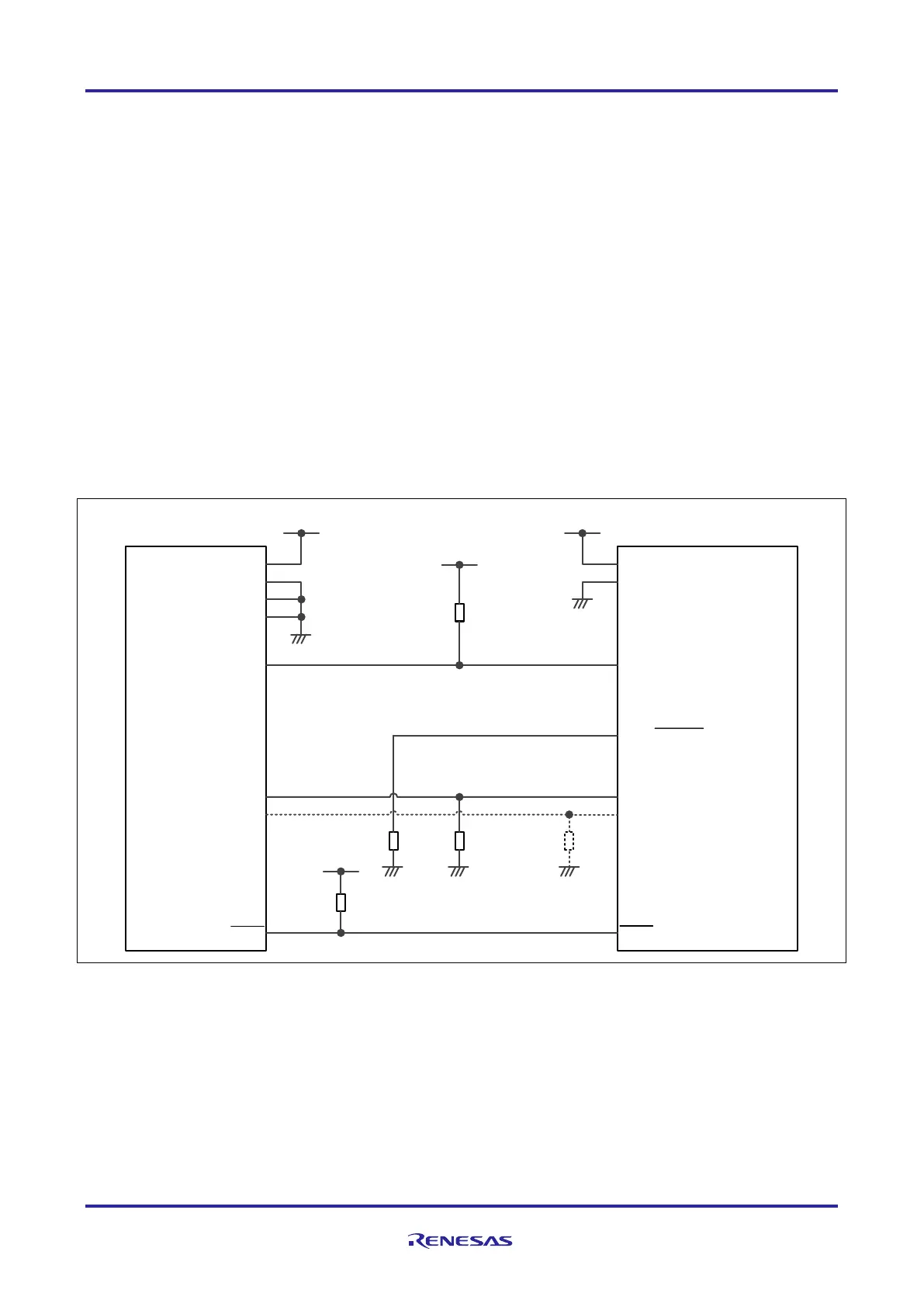
Figure 38: LPD (1 pin) connection
TVDD
GND
GND
GND
VDD
VDD
EVCC
EVSS
TDI/LP DIO
FPM D0
RESET RESET
P10_8 (FLM D1)
No te 2
FLM D0
JP0_0 (DCUTDI/LPD IO, LP DI)
VDD
1k t o 10kΩ
RH850/F1Kx, RH850/F1K
E1/E2 Emulator
(14pin Connector)
Min.
86kΩ
10k to 100kΩ
JP0_4 (DCUTRST)
VDD
No te 1
FPM D1
1k t o 10kΩ

 Loading...


