RH850/F1Kx, RH850/F1K Series Hardware Design Guide
R01AN3841ED0110 Rev. 1.10 Page 41 of 108
August 8, 2019
1.4.4 Power Supply Timing of RH850/F1KH-D8
The RH850/F1KH-D8 has a recommended power supply timing.
The voltage slope of the different power supply pins is defined with min. 0.02V/ms and max. 500V/ms. Satisfy the spec
of voltage slope by using power IC with enable control or by using power IC which starts output over VPOC. The
following shows an example of configuration between RH850/F1KH-D8 and PMIC.
Figure 12: Recommended REG0VCC power configuration for RH850/F1KH-D8
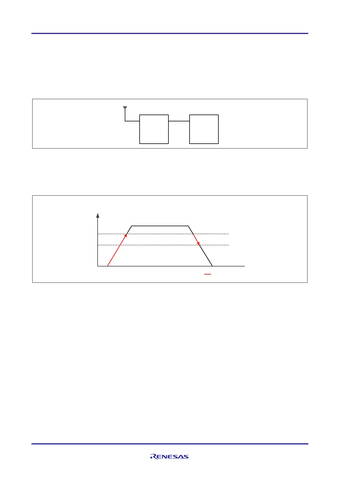
The voltage range which has to be kept voltage slope is as follows. There is no voltage slope limitation at the case other
than below condition. For detail, see the following figure.
Figure 13: The voltage range which has to be kept voltage slope for RH850/F1KH-D8
Note: When the power source rises again, keep the spec of “REGVCC minimum width (t
w_POC
)“ which specified in
the Section 47A.4.5.2, Voltage Detector (POC, LVI, VLVI, CVM) Characteristics of the RH850/F1KH,
RH850/F1KM Hardware User’s Manual.
For details on the electrical characteristics, please refer to Section 47A, Electrical Characteristics of RH850/F1KH-D8
of the RH850/F1KH, RH850/F1KM Hardware User’s Manual.
PMIC
+B
VINx VOUT1
RE G 0V CC
EVCC
RH850/F1KH-D8
: Voltage range that tVS shall be kept
REG0VCC/
REG1VCC/
EVCC/BVCC/
A0VREF/A1VREF
3.0V (VPOC (max))
0V
2.7V (VPOC (min))

 Loading...


