RH850/F1Kx, RH850/F1K Series Hardware Design Guide
R01AN3841ED0110 Rev. 1.10 Page 89 of 108
August 8, 2019
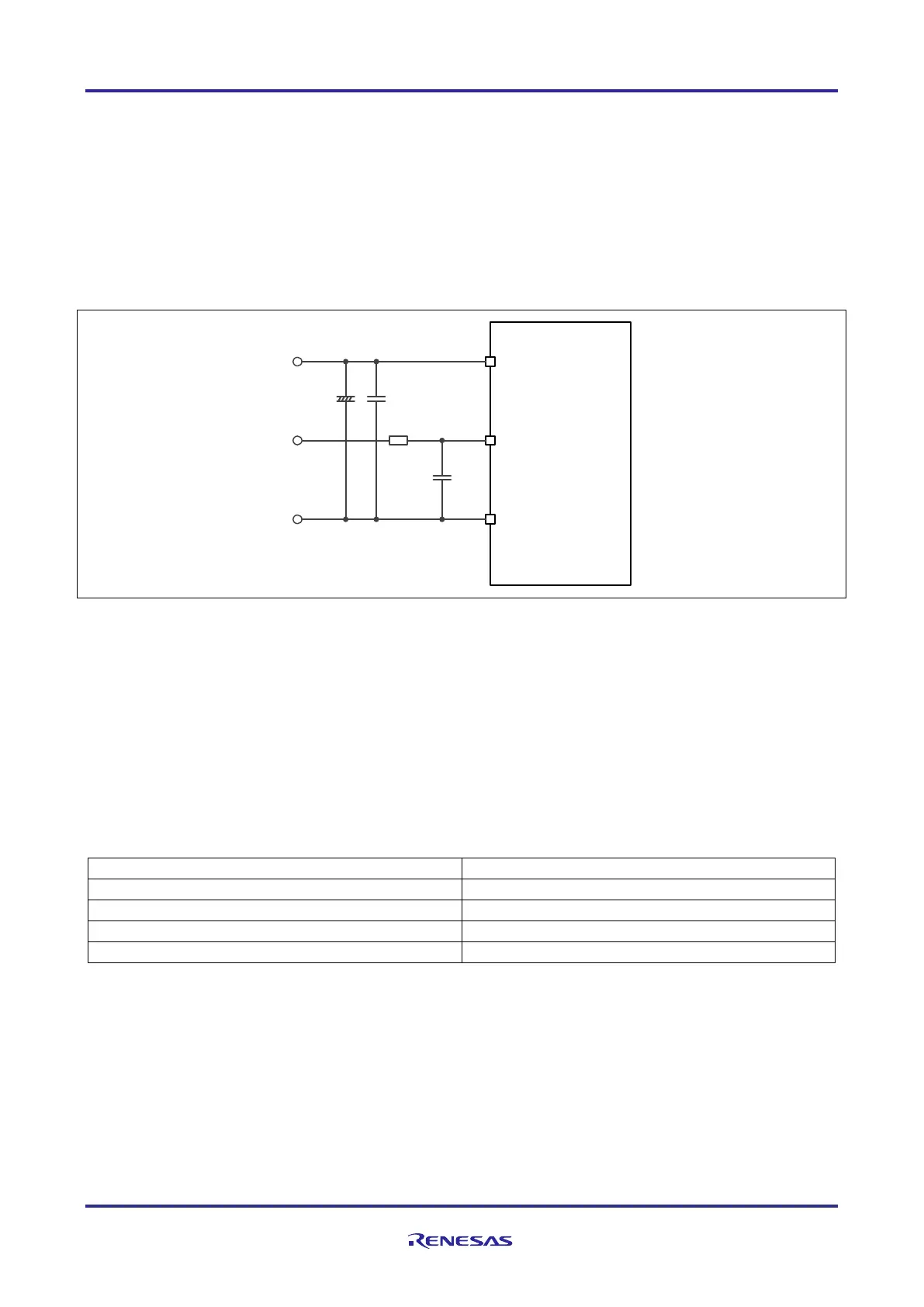
6.4 External Circuit on ADC Input
To preserve the accuracy of the A/D-converter, it is recommended that analog input pins have a low impedance.
Therefore, placing a capacitor at the analog input pin can provide an effective result. This capacitor contributes to noise
filtering on the analog input pin. A basic filter can be realized by using a series resistor with a capacitor on the input pin
(RC-filter).
The filter at the input pins should be designed taking into account the dynamic characteristics of the input signal, the
equivalent input impedance of the ADC itself and the injected current specification of the analog input pins.
Figure 35: ADC external circuit on analog input
For details about suffix “m” and “n”, please refer to Section 38.1.1, Number of Units and
Channels of the RH850/F1KH, RH850/F1KM Hardware User’s Manual or Section 31.1.1,
Number of Units and Channels of the RH850/F1K Hardware User’s Manual.
General guidance values of the basic external ADC input circuit:
Table 67: Basic external ADC input circuit
The values of the resistors and capacitors depend on the application requirements.
The capacitor (C2) placed close to the supply pin AnVREF helps to improve the resistance against electromagnetic
disturbance.
In order to improve the accuracy of the ADC it is recommended to add a capacitor (C1) of minimum 4.7µF in parallel
to the capacitor C2 at AnVREF. The value and PCB placement of the parallel capacitor depends on the application
requirements.
ADCAnIm
RH85 0/F1Kx
Re
Ce
AnVREF
C1
AnVSS
C2

 Loading...


