RH850/F1Kx, RH850/F1K Series Hardware Design Guide
R01AN3841ED0110 Rev. 1.10 Page 91 of 108
August 8, 2019
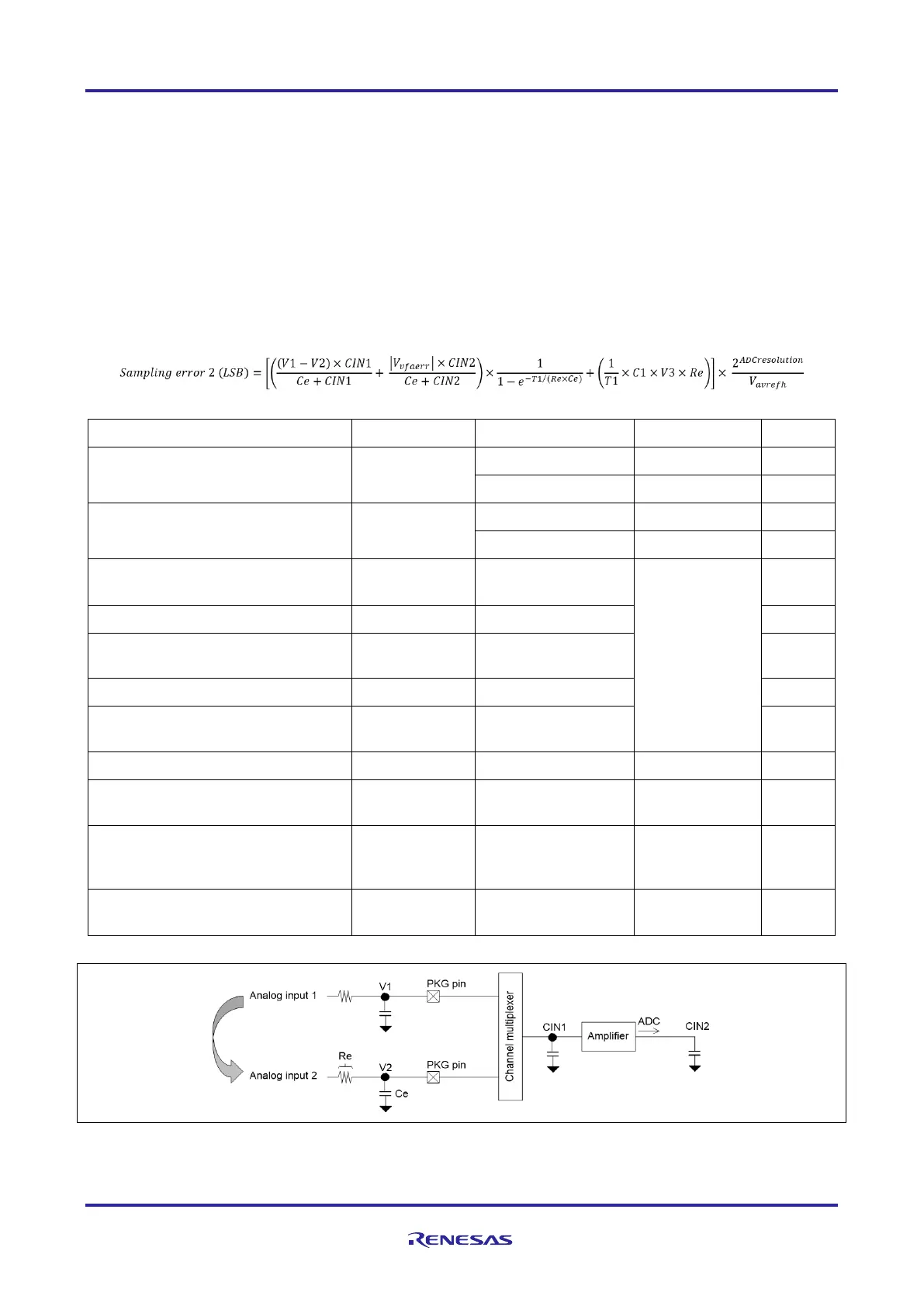
b) Errors (Sampling error 2) which depend on conversion cycles with charge sharing
A formula for errors in sampled values due to the external circuit of the A/D converter is given below. These errors will
depend on the input circuit and conversion cycle. The formula given below for the errors is simplified for the
calculation of sampling error based on internal stray capacitance, amplifier offset, resistance of the signal source, and
conversion cycle. This formula can also be used to calculate the effects of the signal source resistance and conversion
cycle on these errors.
The formula gives the error of analog input 2 as shown in the figure below when A/D conversion is performed in the
order of analog input 1 then 2.
Common capacitance of the final
stage of channel multiplexer
Common capacitance of the final
stage of the amplifier
External capacitor on analog input
pin
customer's
environment
Conversions cycle of analog Input
pins
Potential difference between V1
and V2
Offset voltage of the amplifier
Parasitic capacitance in the
channel multiplexer
|AnVCC voltage / 2.5 - measured
pin voltage (V2)|
customer's
environment
AD-converter resolution, either 12-
bit or 10-bit resolution
Figure 37: Schematic for sampling error 2 formula

 Loading...


