EasyManuals Logo

Renesas RH850/F1Kx Series Hardware Design Guide

Renesas RH850/F1Kx Series
112 pages
To Next Page IconTo Next Page
To Previous Page IconTo Previous Page
Page #87 background imageLoading...
Page #87 background image
RH850/F1Kx, RH850/F1K Series Hardware Design Guide
R01AN3841ED0110 Rev. 1.10 Page 87 of 108
August 8, 2019
6. AD-Converter
6.1 Conversion time
The ADC conversion time consists of a number of timing parameters, which are summed-up to get the conversion
timing depending on the application.
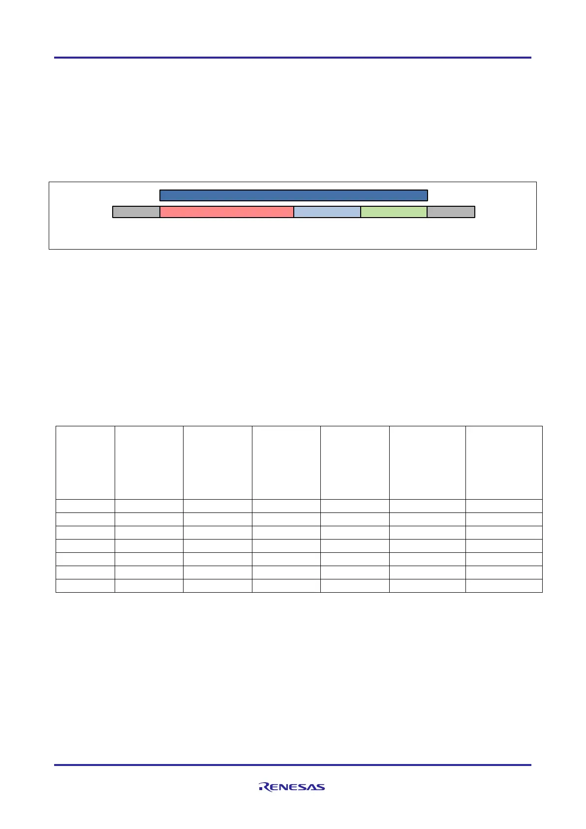
Figure 33: ADC conversion time
Notes:
1.
SG
- Scan Group
2.
MPX
- External multiplexer
3.
HWTRG
- Hardware trigger
4.
SWTRG
- Software trigger
The setting of the ADC clock and the sampling time results in the following conversion timing:
Table 66: ADC conversion time overview
ADCLK
[MHz]
Sampling
time
[clks]
MPX Setup
time
[µs]
Sampling
time
[µs]
Conversion
time
[µs]
Total
conversion
time
(excluding
MPX)
[µs]
Total
conversion
time
(including
MPX)
[µs]
40
24
1.15
0.60
0.55
1.15
2.30
32
18
1.25
0.56
0.69
1.25
2.50
32
24
1.44
0.75
0.69
1.44
2.88
24
18
1.67
0.75
0.92
1.67
3.33
24
24
1.92
1.00
0.92
1.92
3.83
8
18
5.00
2.25
2.75
5.00
10.00
8
24
5.75
3.00
2.75
5.75
11.50
Note: The sampling time is set by the ADCAnSMPCR.SMPT [7:0] bits.
SG setup MPX setup Sampling Conversion
SG end
Total conversion time (single channel)
4c lks HWTRG
9clks SWTRG
Sampling clock + conversion clocks 18cl ks or 24cl ks 6clks22cl ks

Table of Contents

Other manuals for Renesas RH850/F1Kx Series

Questions and Answers:

Question and Answer IconNeed help?

Do you have a question about the Renesas RH850/F1Kx Series and is the answer not in the manual?

Renesas RH850/F1Kx Series Specifications

General IconGeneral
BrandRenesas
ModelRH850/F1Kx Series
CategoryComputer Hardware
LanguageEnglish

Related product manuals