RH850/F1Kx, RH850/F1K Series Hardware Design Guide
R01AN3841ED0110 Rev. 1.10 Page 95 of 108
August 8, 2019
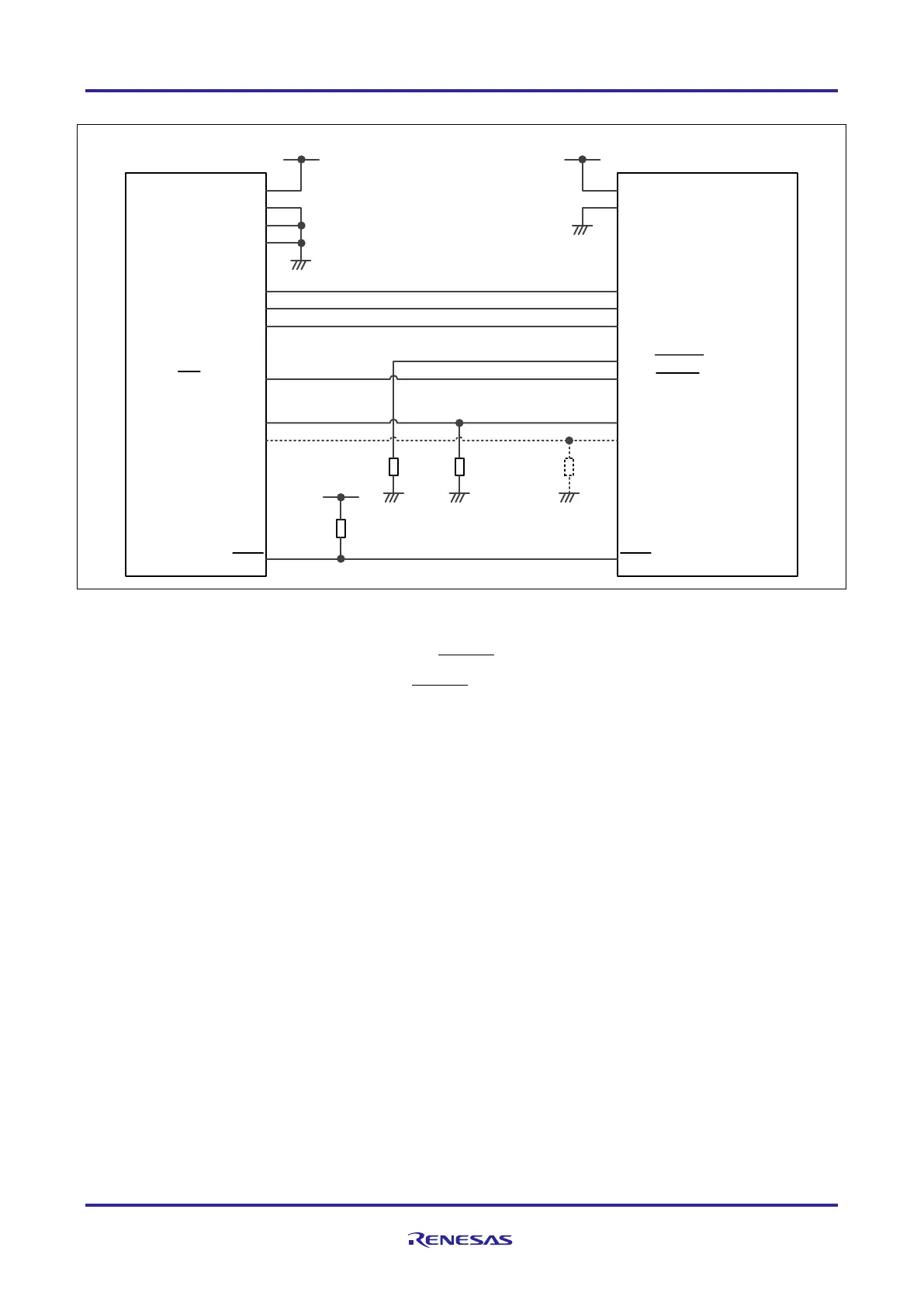
Figure 39: LPD (4 pins) connection
The maximum sink current of the RESET terminal of the E1/E2 emulator is 2mA. The
external pull-up circuit of the
RESET pin has to be considered based on the applications
requirement. When an external RESET component is used, the pull-up resistor value has to be
selected appropriately.
Design the circuit in the way that the FLMD1 pin must be at the low level during serial
programming. During programming (using the RFP), it outputs a low level on FPMD1 to place
the device in the serial programming mode.
If necessary, connect FPMD1 and FLMD1.
When the LPD (4 pins) mode is used, the ports of the JP0 port group are automatically switched to the debug interface
mode. The remaining pins of JP0 can be used as general-purpose I/O pin including its alternate function.
• JP0_0: LPDI input
• JP0_1: LPDO output
• JP0_2: LPDCLK input
• JP0_3: General-purpose I/O
• JP0_4: General-purpose I/O
• JP0_5: LPDCLKOUT output
• JP0_6: General-purpose I/O (depending on device)
TVDD
GND
GND
GND
VDDVDD
EVCC
EVSS
TDI/LP DIO
TDO/LPDO
TCK/LP D CL K
RDY/LP D CL KOUT
FPM D0
FPM D1
RESET RESET
P10_8 (FLM D1)
No te 2
FLM D0
JP0_0 (DCUTDI/LPD IO, LP DI)
JP0_1 (DCUTDO/LPDO)
JP0_2 (DCUTCK/LP D CL K)
JP0_5 (DCURDY /LP DCLKOUT)
RH850/F1Kx, RH850/F1K
E1/E2 Emulator
(14pin Connector)
Min.
86kΩ
1k t o 10kΩ
10k to 100kΩ
JP0_4 (DCUTRST)
VDD
No te 1

 Loading...


