RH850/F1Kx, RH850/F1K Series Hardware Design Guide
R01AN3841ED0110 Rev. 1.10 Page 96 of 108
August 8, 2019
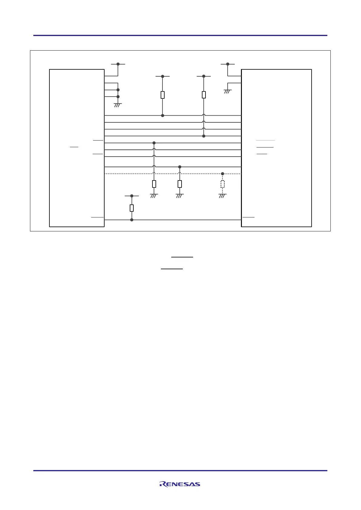
Figure 40: Nexus, LPD (4 pins) and LPD (1 pin) connection
The maximum sink current of the RESET terminal of the E1/E2 emulator is 2mA. The
external pull-up circuit of the
RESET pin has to be considered based on the applications
requirement. When an external RESET component is used, the pull-up resistor value has to be
selected appropriately.
The resistor is optional when the LPD (4 pins) mode is used
The use of an external resistor is only required when the Nexus IF mode is used for debugging
and depends on the hardware specification and implementation of the 3
rd
party development
tool.
When the Nexus interface is used for debugging the value of the resistor depends on the 3
rd
party
development tool specification.
Design the circuit in the way that the FLMD1 pin must be at the low level during serial
programming. During programming (using the RFP), it outputs a low level on FPMD1 to place
the device in the serial programming mode.
If necessary, connect FPMD1 and FLMD1.
TVDD
GND
GND
GND
VDDVDD
EVCC
EVSS
TDI/ LP DIO
TDO/LPDO
TCK/ LPDCLK
TMS
TRST
RDY /LPDCLKOUT
FPM D0
FPM D1
RESET RESET
P10_8 ( FLMD1)
No te 6
FLM D0
JP0_0 (DCUTDI/LPDIO, LPDI)
JP 0_ 1 ( DCUTDO/LPDO)
JP0_2 (DCUTCK/LPDCLK)
JP0_3 (DCUTMS)
JP0_4 (DCUTRST)
JP 0_ 5 ( DCURDY/LPDCLKOUT)
VDD
1k to 10kΩ
No te 2
RH850/F1Kx, RH850/F1K
Emulator
(14pin Connector)
Mi n.
86kΩ
1k to 10kΩ
EVTO
JP0_6 (EVTO)
No te 5
VDD
No te 3
10k to 100 kΩ
No te 4
VDD
No te 1

 Loading...


