RH850/F1Kx, RH850/F1K Series Hardware Design Guide
R01AN3841ED0110 Rev. 1.10 Page 90 of 108
August 8, 2019
As guide line for the calculation of the external capacitor at the analog input pin the formula based on the internal
equivalent capacitance and the ADC resolution of the corresponding AD-converter channel can be used. In this case,
sampling error based on charge-sharing between Ce and CIN will be roughly 1 LSB at the start timing of sampling.
= × 2
Ce: External capacitor at the analog input pin
CIN: Equivalent input capacitance
ADCresolution: AD-converter resolution for RH850/F1Kx or RH850/F1K, either 12-bit or 10-bit resolution
6.5 Formulas for sampling error
Sampling error is error to which “Errors (Sampling error 1) which depend on input leakage current of analog pin” and
“Errors (Sampling error 2) which depend on conversion cycles with charge sharing” were added.
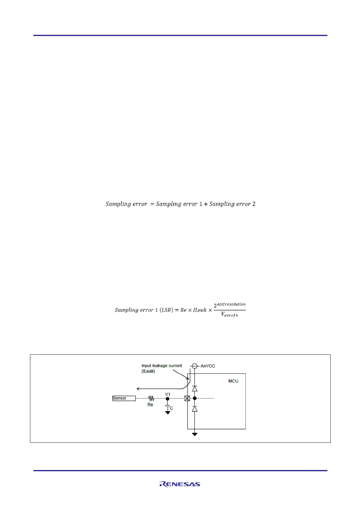
The external circuit of the A/D pin indicates below about the factor (sampling error 1 and sampling error 2) which
becomes sampling error.
a) Errors (Sampling error 1) which depend on input leakage current of analog pin
The error depends on the input leakage current (ILeak) of analog pin and external resistance (Re), and occurs. The error
which depends on the input leakage current is given by the formula of the following.
Vavrefh: AnVREF voltage
ADCresolution: AD-converter resolution for RH850/F1Kx, either 12-bit or 10-bit resolution
Figure 36: Schematic for sampling error 1 formula

 Loading...


