Response times for analog input device and output device
F.2 Response times for analog output device
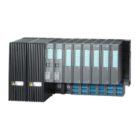
ET 200eco PN
Operating Instructions, 08/2016, A5E01250250-AJ
259
Response times for analog output device
Conversion time
The conversion time of the analog output channels includes the transfer of digitized output
values from internal memory, and their digital-to-analog conversion.
The analog output channels are converted for the device with an execution time plus the
sequential conversion time for channels 0, 1, 2, and 3.
The cycle time, i.e., the time until an analog output value is converted again, is the sum of
the conversion times of all the activated analog output channels and of the processing time
of the analog output device. You should deactivate unused analog output channels during
parameter assignment in order to reduce the cycle time. The conversion time for a
deactivated channel is 0 ms.
The following figure provides you with an overview of the cycle time elements for an analog
output device.
Figure F-2 Cycle time of analog output modules
The settling time (t
2
to t
3
)—that is, the time from the application of the converted value until
the specified value is reached at the analog output—depends on the load. We therefore
distinguish between resistive, capacitive, and inductive loads.
 Loading...