MicroBlaze Processor Reference Guide 33
UG984 (v2018.2) June 21, 2018 www.xilinx.com
Chapter 2: MicroBlaze Architecture
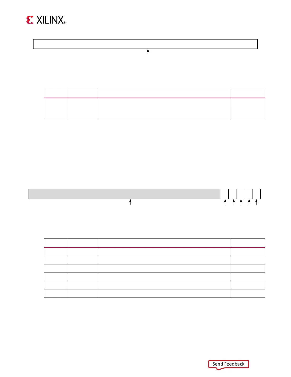
Floating-Point Status Register (FSR)
The Floating-Point Status Register contains status bits for the floating-point unit. It can be
read with an MFS, and written with an MTS instruction. When read or written, the register is
specified by setting Sa = 0x0007. The bits in this register are sticky − floating-point
instructions can only set bits in the register, and the only way to clear the register is by
using the MTS instruction. The following figure illustrates the FSR register and
Table 2-14
provides bit descriptions and reset values.
X-Ref Target - Figure 2-7
Figure 2-7: BTR
Table 2-13: Branch Target Register (BTR)
Bits Name Description Reset Value
0:31 BTR Branch target address used by handler when returning from
an exception caused by an instruction in a delay slot.
Read-only
0x00000000
X-Ref Target - Figure 2-8
Figure 2-8: FSR
31
DO
Reserved
3029
27
UFOF
DZIO
28
0
X19745-091317
Table 2-14: Floating-Point Status Register (FSR)
Bits Name Description Reset Value
0:26 Reserved undefined
27 IO Invalid operation 0
28 DZ Divide-by-zero 0
29 OF Overflow 0
30 UF Underflow 0
31 DO Denormalized operand error 0